
Skip to content
HARDWARE · HARDWARE / FABRICATION METROLOGY

A sidewall protocol puts qubit fabrication under a more consistent microscope

A scanning-probe study defines how to measure etched device edges. The contribution is a reproducible measurement method, with the link to qubit lifetime still to establish.
Published Source report Sources checked
My reading list
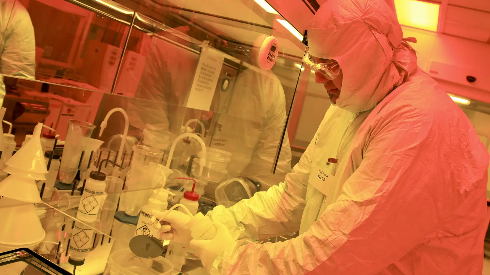
Scientist rinsing a silicon-on-insulator wafer while fabricating photonic circuits in a cleanroom
A scientist works with a wafer in Oak Ridge National Laboratory’s CNMS cleanroom. Archival fabrication context; this is not the tantalum sidewall sample or metrology experiment described in the preprint.Photo: ORNL · CC BY 2.0 · CC BY 2.0Full image credit

What changed

A new preprint proposes a common way to measure the etched edges of components. The team uses scanning-probe microscopy to describe lateral roughness and vertical shape, then applies its procedure to fabricated devices. The intended gain is comparability: a geometric descriptor should mean the same thing across measurements.[1]

The method keeps the instrument inside the result. Probe shape limits which features can be resolved, so the authors recommend reporting probe geometry alongside the descriptor. Their protocol also records sample tilt, scan direction, filtering and uncertainty. Section IV and its first two tables collect the practical requirements.[1]

What the result establishes

This is measurement research rather than a demonstration of longer-lived qubits. The authors explicitly reject treating roughness as a universal, direct measure of superconducting quality. Establishing a statistically useful relationship with device performance needs further work on competing loss mechanisms and the conditions under which each matters.[1]

For a reader evaluating a fabrication claim, the useful question is therefore more specific than whether a chip looks smoother. Were the samples examined with comparable probes and analysis settings? A difference between two reported numbers can reflect a changed measurement procedure as well as a changed manufacturing process.

One helpful next experiment would give multiple laboratories shared samples and a fixed analysis protocol, then compare their results before revealing sample identities. That is QubitWire’s suggested follow-up, not an experiment reported in this paper. A separate study would then need to connect those measurements with electrical performance.

The next useful test

The preprint supplies a way to make that investigation better defined. Readers can use its protocol as a checklist for what a future manufacturing comparison should disclose. Improved measurement consistency and improved coherence answer different questions; the present result advances the first without establishing the second.

Keep your reading trail

Your Updates →

Evidence & context

1 linked source

Research preprint

How to read the evidence and dates

An announcement records what an organization stated. An experiment reports an observation. A simulation or resource estimate depends on its assumptions. QubitWire’s analysis connects these sources; the labels are not quality scores.

Published is the article’s first QubitWire publication. Updated marks a substantive content change. Sources checked records a review of the underlying evidence. An older paper can support a new explanation, and another press release about the same work is not independent replication.

QubitWire take

Metrology and fabricated-device characterization are demonstrated; a universal predictor of coherence or yield is not established.

Sources

  1. Sidewall Metrology Protocol for Superconducting Qubit Devices — version 1

    Preprint dated 2026-10-19. Reviewed 2026-10-20: Section II.3: geometrical descriptors; Section II.4: probe geometry and resolution limits; Section IV, Tables 1 and 2: measurement protocol and variability; Section VI: sample fabrication, probe, instrumentation and processing. Methods and limitations checked; no independent reproduction.

READ NEXT

Continue exploring

All Hardware stories
  1. Explore chip manufacturing

    The U.S. Is Betting Up to $375 Million on Quantum’s Factory Problem

    A milestone-based GlobalFoundries award puts fabrication, packaging and domestic supply chains at the center of the quantum race.

    Published · Source report · Sources checked
  2. Explore chip manufacturing

    A compact visible-light chip must survive the fabrication window

    Recent context from October 8–12: fabricated visible-light components illustrate why inverse design must include manufacturing tolerance.

    Published · Source report · Sources checked
THE QUANTUM BRIEFING

A clearer signal.
Read the latest edition.

A little perspective on a fast-moving field.

Read the on-site briefing →

Read selected quantum coverage in the on-site briefing, or register your interest below.