
Wolfspeed’s transparent wafer opens a new test for quantum hardware
Wolfspeed has introduced optical-grade silicon carbide. Its promise will be tested in the devices researchers build from it.
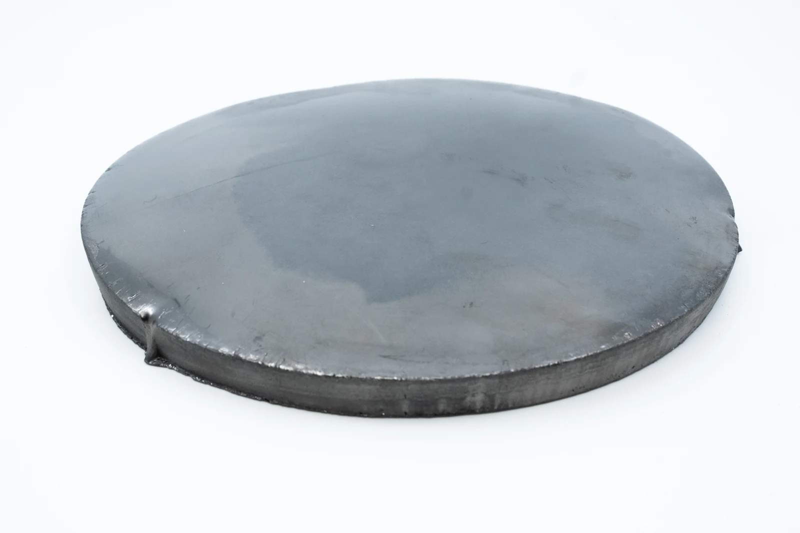

Wolfspeed has introduced a transparent wafer for markets that include quantum computing. On October 29, the company launched TSiC, its optical-grade silicon carbide technology, with augmented reality among the other target uses. The launch supplies a new starting material. The interesting question is what researchers can build from it and how well those devices will work.[1]
Why a clear crystal matters
Silicon carbide combines silicon and carbon in a crystal. Particular defects in its atomic arrangement can host controllable spins, offering a way to hold quantum information. A study published online in 2014 demonstrated coherent control of an individual silicon-vacancy spin at room temperature. That history helps explain why quantum engineers are interested in this material.[4]
Another study, published in Nature Communications in 2024, integrated an electron-nuclear spin register into a silicon-carbide photonic waveguide. A waveguide provides a defined path for light. Putting a quantum element beside that path is one route toward connecting its state to an optical circuit. This older experiment establishes research context; it did not test the new TSiC product.[3]
The appeal is the possibility of giving one material several jobs. A substrate can support a device, guide light through a fabricated structure or host the defect used as a quantum element. Those jobs have different requirements. A material that works well as mechanical support still needs separate evidence before it can serve as a useful host.[2]
What is available now
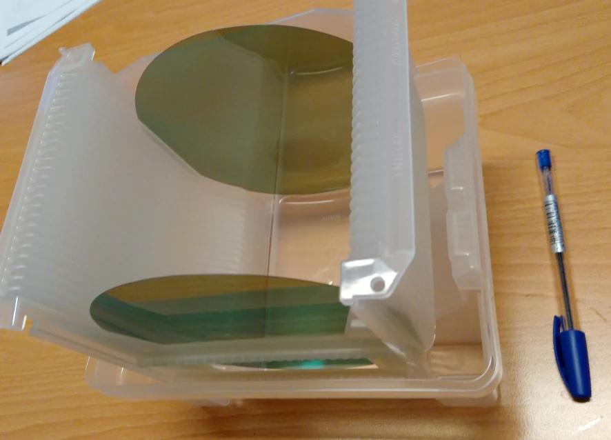
Wolfspeed's product page lists 150 mm and 200 mm wafers as commercially available. It describes 300 mm material as sampling and available on request, while the launch announcement says the largest format remains under development. Buyers should read those descriptions together rather than assume that every size has reached the same production stage.[1][2]
The supplier gives target optical and dimensional specifications and says they may vary by diameter. These specifications describe the starting material under stated conditions. They are useful for planning an evaluation, but a finished quantum device introduces additional steps and additional ways for performance to change.[2]

From material to working device
A larger wafer offers more area to work with. The useful output, however, depends on how many fabricated devices meet their requirements. An evaluation should track variation across the wafer, the proportion of usable devices and consistency between batches. These are proposed checks for researchers and buyers, not measurements supplied by this announcement.
Transparency also needs a precise question attached to it. Light crossing a sample and light traveling through a complete circuit are different tests. The circuit may include bends, etched surfaces and connections to other parts. Measuring the finished route would show whether the initial optical properties survive the process needed to make a useful component.
Consider a research team choosing between two substrates. One has a stronger optical specification but requires an unfamiliar fabrication process. The other offers less impressive headline numbers and a process the team already understands. The choice depends on the intended experiment, development effort and acceptable failure rate. This hypothetical comparison shows why a single material specification cannot settle a system decision.
The result to watch next
For a defect-based device, an informative follow-up would identify the material and processing history, then test preparation, control and measurement of the intended quantum state after fabrication. Repeating that experiment on independently prepared samples would help distinguish a promising example from a dependable route. QubitWire has not performed those tests.
There is a supply question alongside the physics question. A research sample, a qualified part and a repeatable production order meet different needs. A buyer would need clear acceptance criteria for the chosen diameter and a way to compare batches. Availability opens that conversation; it does not reveal the delivered yield of a future customer's design.
Wolfspeed's announcement matters at the beginning of the engineering process: obtaining material that can be specified, processed and tested. The next meaningful evidence will connect that starting wafer to a reproducible device result. That is the point where an attractive material becomes a demonstrated solution to a quantum hardware problem.