
A chipmaking ingredient gets a new job in quantum readout
A Nature Electronics paper published November 4 turns an existing chip material into a compact sensing component. The study was first preprinted in July 2025; spin-qubit readout is the next test.
Reading tools for text size, copying, printing and your reading list
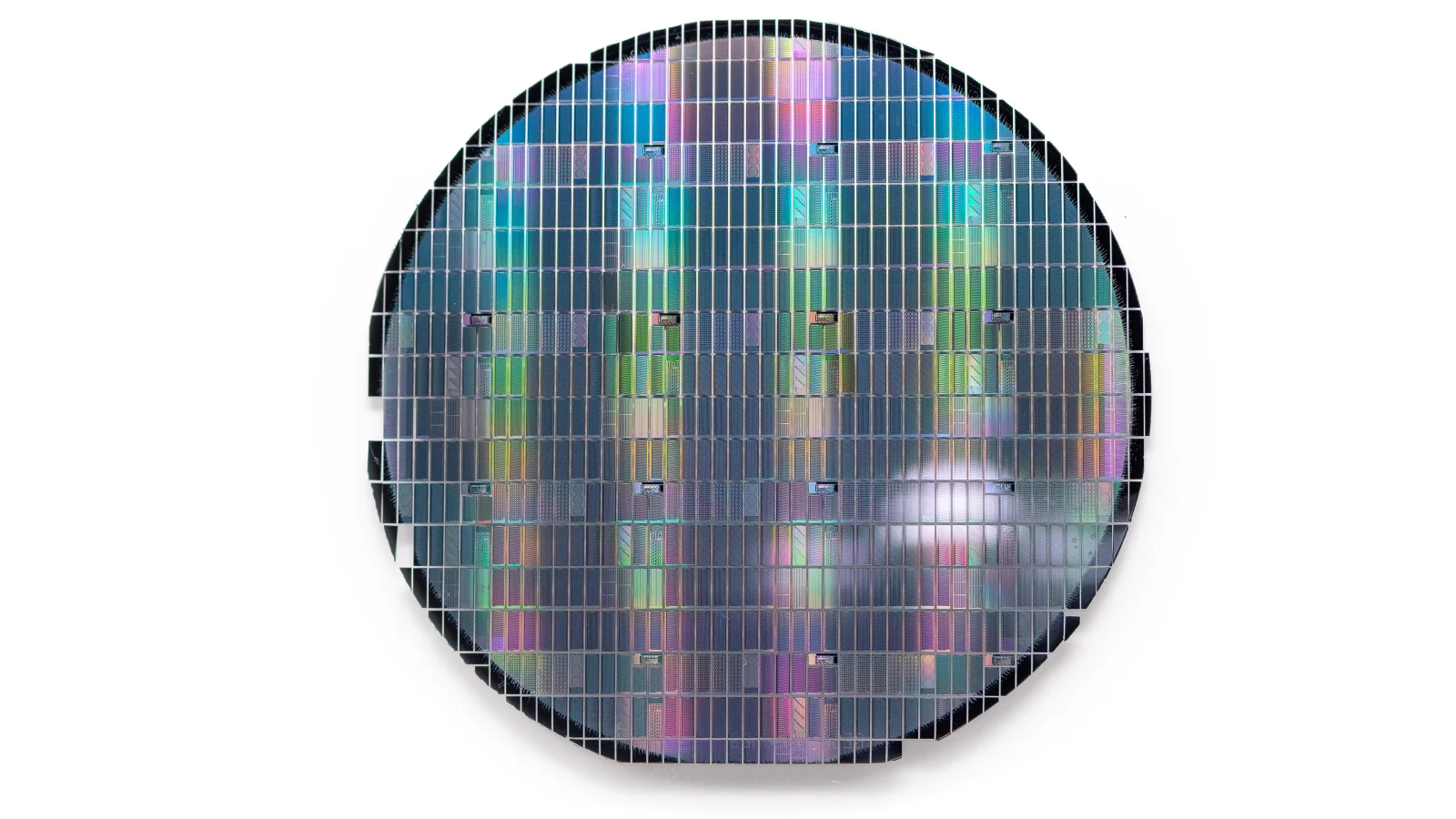
Building a quantum device is only part of the job. The equipment that reads its state also has to fit somewhere. In a paper published in Nature Electronics on November 4, researchers used titanium nitride already available in a commercial silicon manufacturing process to make an unusually compact superconducting circuit element. They combined it with a quantum dot on the same chip to form a sensitive charge sensor.[1][2]
The practical attraction is integration: more of the listening hardware can be made together. High-fidelity spin readout is a next step, rather than a result this experiment has already delivered.[1][2]
A familiar material, used in the cold
The process is GlobalFoundries’ 22-nanometre fully depleted silicon-on-insulator technology. The researchers exploit a property of its titanium nitride film when superconducting: a large kinetic inductance. Their circuit element is a superinductor, a name that refers to its unusually high intrinsic impedance.[1]
An ordinary way to make an inductor is to arrange a conductor into a coil. In this case, the useful inductive response comes from the superconducting material itself. The manufacturing idea is attractive because a component can gain a new function without requiring the entire chip to be built around an unfamiliar fabrication process. That is an engineering opportunity to test, not a guarantee of low cost or mass-production yield.[3]
The sensor and the thing it senses
A quantum dot confines electric charge in a small region. Coupling it to the resonant circuit allows a changing electrical response to be detected with a radio-frequency signal. Both the preprint and the journal article describe the integrated sensor and its nonlinear circuit behavior. The current milestone is publication of the peer-reviewed account.[4][1]
There is a useful distinction between detecting a charge response and reliably reporting the state of a spin . A sensor can be an essential ingredient in that readout chain without completing every step. The nanoGUNE announcement explicitly identifies integration with multigate transistors for fast, high-fidelity spin readout as future work.[2]
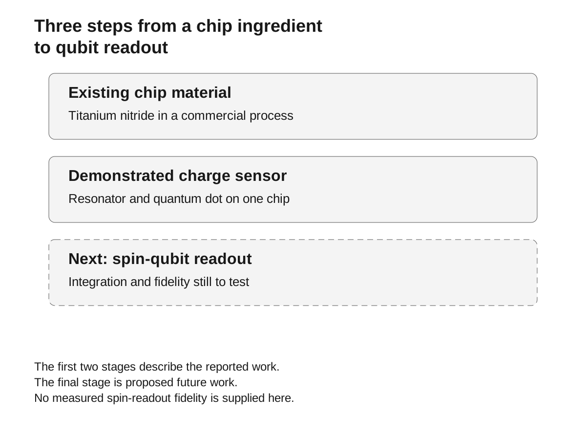
Read this graphic in text
- Existing material: titanium nitride in a commercial chip process.
- Demonstrated: a resonator and quantum dot on one chip used for charge sensing.
- Future test: integrated spin-qubit readout and its accuracy.
The final stage is proposed work. The study does not supply a measured spin-readout fidelity.
Read the component number at the right scale
The paper describes an 18-square-micrometre inductor structure. That is a component footprint, not the area of the complete chip or a future quantum computer. Its sensitivity measurements also concern the tested sensor conditions. They should not be relabeled as a qubit error rate, a processor speed, or an application speedup.[1]
A component number is most helpful when its boundary is visible. Imagine a floor plan in which one room becomes much smaller. The building may gain useful space, but that improvement does not tell you the new size of every corridor, the capacity of the plumbing or the cost of the whole project. A chip has its own version of those integration questions.
Why the manufacturing connection matters
The same-day News & Views article by Thaddeus D. Ladd highlights the prospect of using material from an existing gate stack for compact sensing. It is expert interpretation of the work, not an independent rerun of the experiment. The underlying manuscript was already available as a July 2025 preprint, so the fresh event is its journal publication and accompanying explanation.[3][4]
The next useful evidence would connect the compact resonator to the intended qubit readout, report the accuracy under the same operating conditions, and show what happens when more devices share the surrounding circuitry. For manufacturing, consistency across devices would be as informative as the performance of a particularly good one. Those are follow-up questions proposed here, not results claimed by the team.
The story is a reminder that scaling quantum hardware involves the parts around the qubit as well as the qubit itself. An existing chip ingredient has acquired a promising additional job. Now the experiment has to show how well that job fits into the larger machine.