
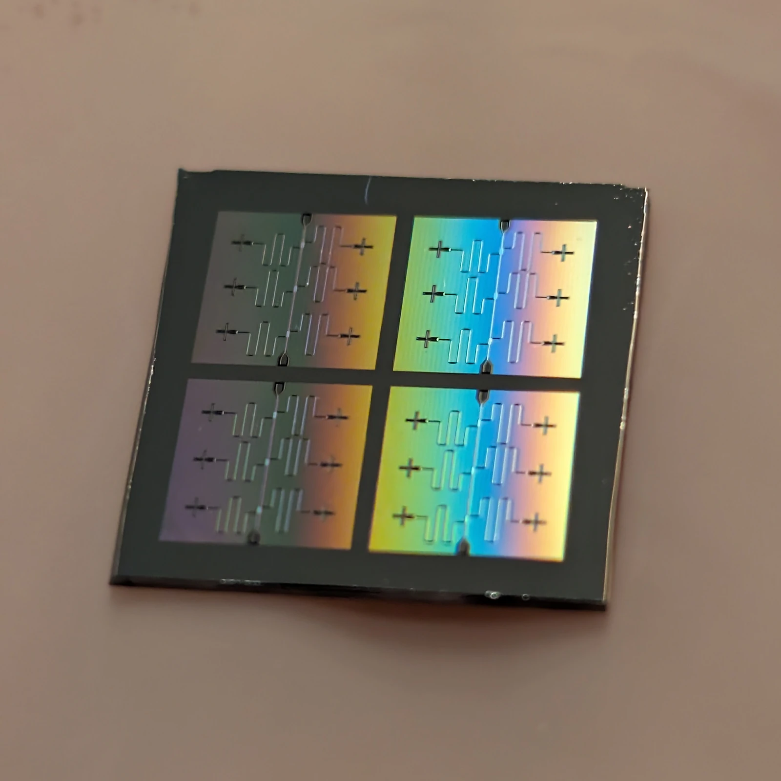
A patterned transmon chip before packaging
The chip is small enough to fit comfortably in a hand, yet the photograph contains several different engineering stories. Repeated patterns show that fabrication starts with a layout, while the uncovered surface makes this a useful counterpart to a packaged device. The source identifies the fabrication tools used; the picture itself cannot establish coherence, yield or successful operation. Ask what measurements would be required after fabrication and which would have to wait until the device is cooled. This is an introduction to the distance between making a pattern and demonstrating a reliable qubit.
- Organization
- OJB Quantum
- Image type
- Photograph
- Capture date
- 2026-08-02
- Photographer / creator
- OJB Quantum
- Reuse terms
- CC BY 4.0
OJB Quantum — 24 Transmon Qubits Patterned by Direct Write LASER Lithography.jpg — CC BY 4.0 — https://commons.wikimedia.org/wiki/File:24_Transmon_Qubits_Patterned_by_Direct_Write_LASER_Lithography.jpg — https://creativecommons.org/licenses/by/4.0.
Full original frame retained; EXIF orientation normalized where present, resized without enlargement and converted to WebP. No crop or content alteration.
Read the image
Read a patterned surface as a fabrication object
Begin with the repeated shapes, then look at the reflections. The photograph shows a physical patterned chip whose apparent colors depend on its surface and the lighting. Those colors help the eye follow regions of the device, but they are not a map of temperature, qubit state or measured quality.
The source identifies transmon fabrication work. That context makes the picture useful for explaining the first stage of an experimental device: a design has been realized as material structure. Later stages include mounting, connecting, cooling and measuring. Each supplies a different kind of evidence.
Keep the distinction between a visible pattern and a functioning element explicit. A repeated feature can be located in an image without proving its electrical response. The next useful document would be a fabrication description or a characterization result linked to the same device, rather than a performance number borrowed from a different processor.
What is directly visible?
A square chip, repeated patterned regions and iridescent reflections. Their dimensions and electrical behavior are not established by this view.
Why retain the full frame?
It preserves the relationship among patterned areas. A decorative crop could hide the repetition that gives the image its educational purpose.
What would establish device performance?
A defined measurement with operating conditions, analysis and device identity. A component count in a filename is not that measurement.
An independent QubitWire lesson based on this image and the cited source reading. The image does not establish a performance result.
Keep exploring
More from the same organization or hardware architecture.
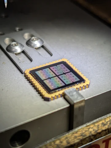 The package around a transmon chipOJB Quantum · CC BY 4.0
 Quantum System One at ThinkLabOnri Jay Benally (OJB Quantum) · CC BY 4.0
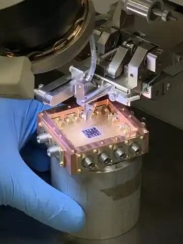 Inside an AQT processor packageAdvanced Quantum Testbed/Berkeley Lab · NQI gallery reuse permission
 Inside the SQMS Quantum GarageRyan Postel / Fermilab · NQI gallery reuse permission
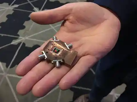 Three qubits in the palm of a handAnita Fors (Chalmers) · CC BY-SA 4.0
 Sycamore on displayColdupnorth · CC BY-SA 4.0
Back to all images · Explore the interactive Model · Image rights and corrections