
Quantum in pictures
Where a patterned chip becomes an experimental device
Two photographs from August 2026 make the transition from a fabricated pattern to its surrounding package easier to follow.
Research context: October 19, 2026 · Source review: October 20, 2026
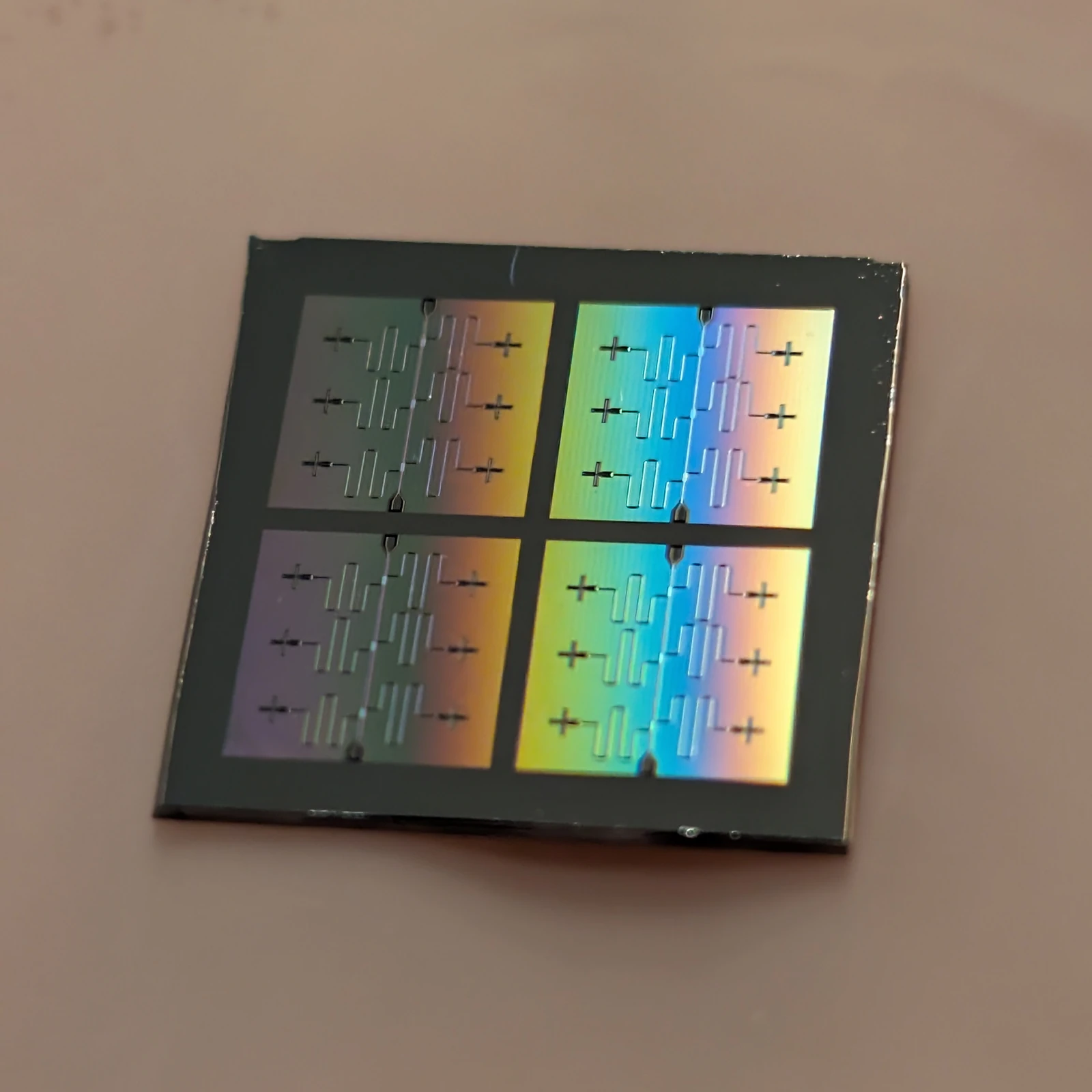
The chip is small enough to fit comfortably in a hand, yet the photograph contains several different engineering stories. Repeated patterns show that fabrication starts with a layout, while the uncovered surface makes this a useful counterpart to a packaged device. The source identifies the fabrication tools used; the picture itself cannot establish coherence, yield or successful operation. Ask what measurements would be required after fabrication and which would have to wait until the device is cooled. This is an introduction to the distance between making a pattern and demonstrating a reliable qubit.
OJB Quantum — 24 Transmon Qubits Patterned by Direct Write LASER Lithography.jpg — CC BY 4.0 — https://commons.wikimedia.org/wiki/File:24_Transmon_Qubits_Patterned_by_Direct_Write_LASER_Lithography.jpg — https://creativecommons.org/licenses/by/4.0.Full original frame retained; EXIF orientation normalized where present, resized without enlargement and converted to WebP. No crop or content alteration.
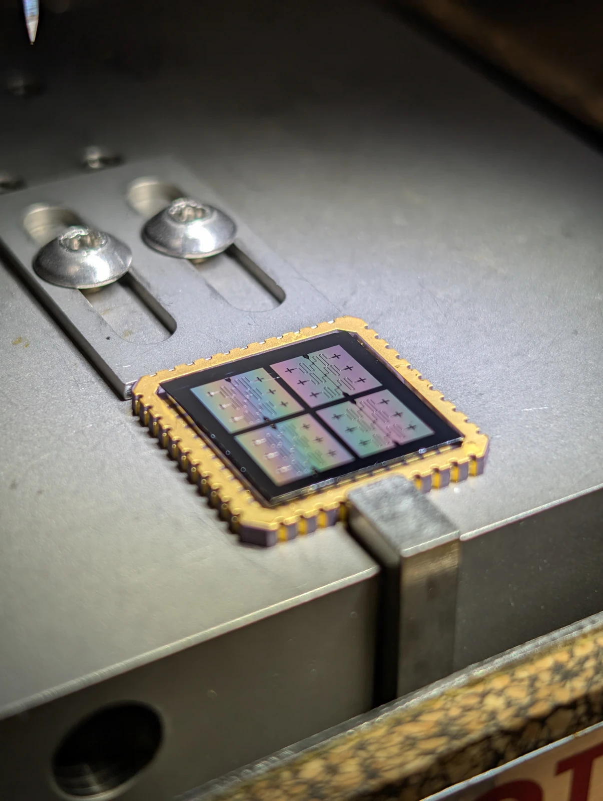
A package creates a practical boundary between a delicate chip and the equipment that will operate it. Here the source describes a patterned chip resting on a package used with wire bonding. The surrounding metal and tools give a stronger sense of scale than an isolated product image. Do not describe visible positioning as completed electrical assembly: this photograph does not establish which connections have been made or tested. Use it to explain the questions a package must answer, including how the chip is supported, how signals reach it and how the completed assembly will be inspected.
OJB Quantum — 24 Transmon Qubits Patterned by Direct Write LASER Lithography 003.jpg — CC BY 4.0 — https://commons.wikimedia.org/wiki/File:24_Transmon_Qubits_Patterned_by_Direct_Write_LASER_Lithography_003.jpg — https://creativecommons.org/licenses/by/4.0.Full original frame retained; EXIF orientation normalized where present, resized without enlargement and converted to WebP. No crop or content alteration.
One photograph presents a square patterned chip almost as an abstract surface. Gold, blue and dark reflections divide the frame into repeated regions. In the second view, the same source’s device sits within a gold-colored package, with the work surface and nearby handling context visible. OJB Quantum identifies both photographs as transmon-chip fabrication work and dates them to August 2, 2026.[1][2]
The useful story is the change of context. A patterned surface shows that fabrication has produced a physical object. A package begins to show how that object can be held and connected as part of an experiment.
These are related engineering stages, but neither photograph by itself reports the outcome of a qubit measurement. The source filename’s device count should remain an attributed description rather than become a claim that every pictured element has demonstrated a particular performance.
A transmon is a superconducting circuit used as a quantum bit. Its intended behavior depends on the electrical structure being fabricated, while its measured behavior also depends on how the device interacts with its surroundings. The same separation appears throughout experimental engineering: a design specifies what should happen, manufacture creates an object intended to realize it, and characterization tests what the object actually does.
IBM’s account of its own characterization laboratory provides a separate, concrete example of that final stage. In the laboratory described in December 2024, researchers cooled chips and measured properties including qubit frequency, coherence and coupler tuning before deployment. That is evidence about IBM’s testing process, not evidence that the OJB Quantum chip passed those tests or was made by IBM. The example gives readers a vocabulary for the questions that follow fabrication.[3]
Frequency asks where a device responds under a specified measurement. Coherence concerns how long relevant quantum information remains usable under the chosen conditions. Coupler characterization examines how interactions can be controlled. Each question requires an experiment and a defined interpretation. A photograph can help a reader locate the object under test, but it cannot supply the measurements or replace the conditions written beside them.
The package view is a good place to introduce interfaces. A chip has to exchange signals and heat with equipment around it while maintaining the environment needed for operation. Connections are therefore part of the experimental design, not merely a way to make the finished object convenient to hold. An original diagram can follow this progression from patterned device to mounted device to cold test, with separate output boxes for measured frequency, coherence and interaction behavior.
The two photographs deserve to be seen together because the second answers a question raised by the first: where does this small object go next? The answer is an experimental system, followed by evidence about its behavior. That sequence gives the images a purpose beyond their visual appeal. Readers can appreciate the pattern and the package while learning to look for the measurements that turn a plausible device into a characterized one.[1][2][3]
Three stages and the evidence each one supplies
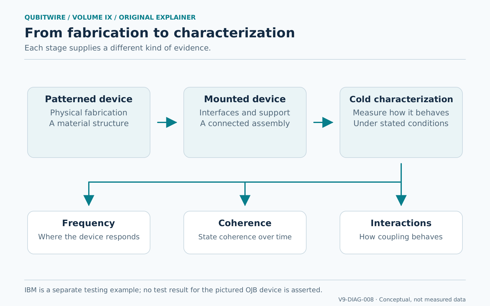
Three stages show a patterned device, a mounted device and cold characterization. The first establishes physical fabrication; the second adds interfaces and support; the third produces measurements such as frequency, coherence and interaction behavior. The OJB photographs show fabrication and packaging, while IBM’s laboratory is a separate explanatory testing example.
Conceptual explanation; not an apparatus construction drawing or a measured result. Original QubitWire explanatory diagram.
Sources and further reading
- 24 Transmon Qubits Patterned by Direct Write LASER Lithography ↗OJB Quantum / Wikimedia Commons
Photographed patterned chip, source description, August 2, 2026 metadata and CC BY 4.0.
- 24 Transmon Qubits Patterned by Direct Write LASER Lithography 003 ↗OJB Quantum / Wikimedia Commons
Separate package-context photograph of the source’s device, same date and license.
- How to test a quantum computer chip ↗IBM Research
Separate IBM example of cold characterization measurements before deployment.