
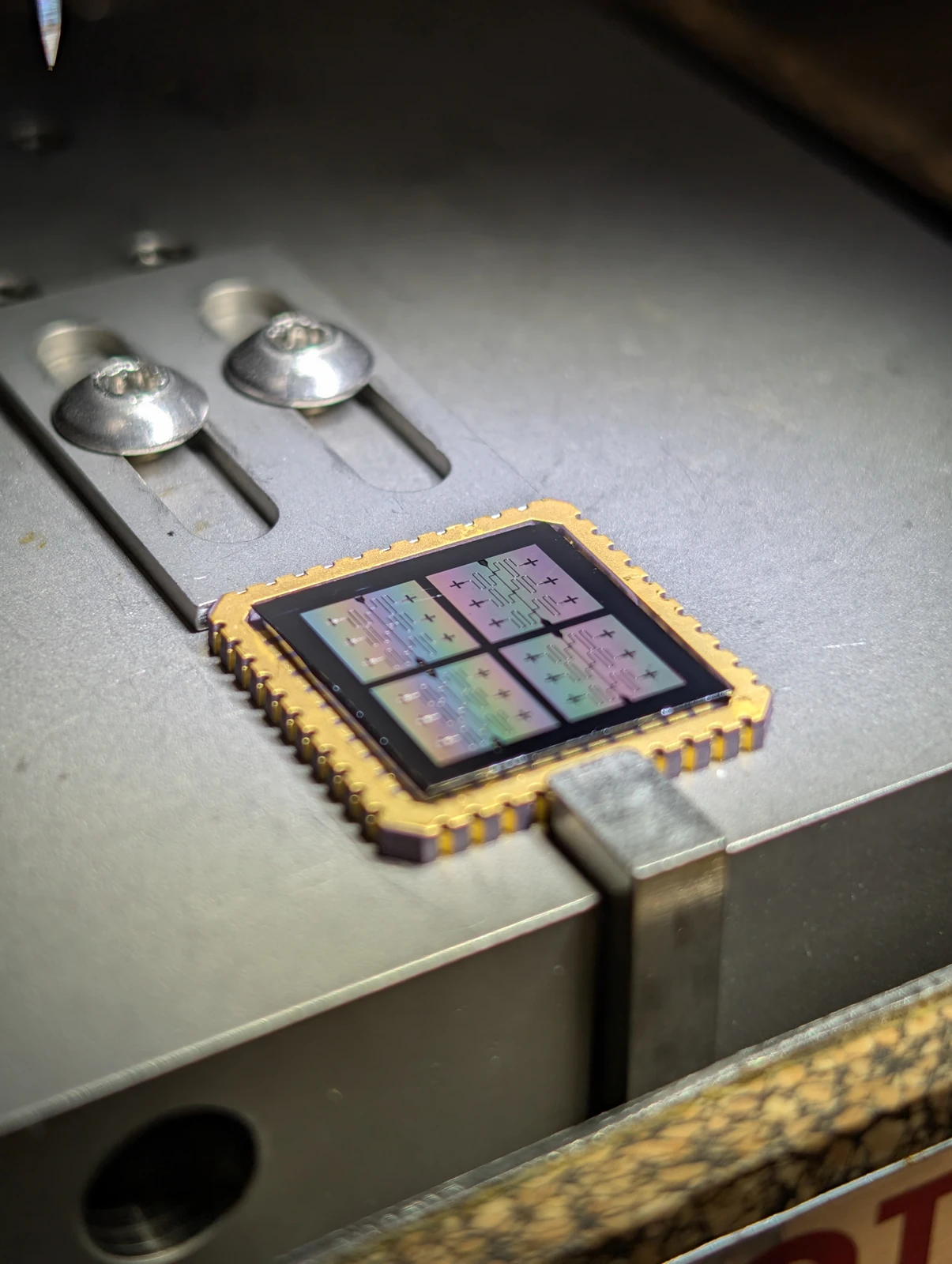
The package around a transmon chip
A package creates a practical boundary between a delicate chip and the equipment that will operate it. Here the source describes a patterned chip resting on a package used with wire bonding. The surrounding metal and tools give a stronger sense of scale than an isolated product image. Do not describe visible positioning as completed electrical assembly: this photograph does not establish which connections have been made or tested. Use it to explain the questions a package must answer, including how the chip is supported, how signals reach it and how the completed assembly will be inspected.
- Organization
- OJB Quantum
- Image type
- Photograph
- Capture date
- 2026-08-02
- Photographer / creator
- OJB Quantum
- Reuse terms
- CC BY 4.0
OJB Quantum — 24 Transmon Qubits Patterned by Direct Write LASER Lithography 003.jpg — CC BY 4.0 — https://commons.wikimedia.org/wiki/File:24_Transmon_Qubits_Patterned_by_Direct_Write_LASER_Lithography_003.jpg — https://creativecommons.org/licenses/by/4.0.
Full original frame retained; EXIF orientation normalized where present, resized without enlargement and converted to WebP. No crop or content alteration.
Read the image
The package begins the connection to the rest of the experiment
The package view changes the scale of the story. A small patterned chip now sits inside a larger gold-colored support, with a work surface and tools nearby. The photograph gives a reader a place to ask how an experimental chip will be held, connected and handled.
Packaging creates interfaces between a device and its surroundings. In a quantum experiment, those interfaces must support the intended signals and environment while avoiding unwanted interactions. The photograph identifies a physical arrangement, but it does not reveal the function of every connection or show that the assembly is ready for operation.
Use this image after the patterned-surface view. The sequence explains a progression from fabrication to integration without pretending that the two photographs contain the entire manufacturing record. A later cold-test photograph or a linked measurement report would supply a different stage of the evidence.
What changes between the two views?
The surrounding package and handling context become visible. The new information concerns integration and scale, not an automatically improved qubit specification.
Can the metal color establish the material?
No. Appearance alone is insufficient for a material identification; use the source’s verified fabrication documentation for that claim.
Why avoid naming every visible connection?
A photograph may not reveal its electrical or thermal purpose. Incorrect labels can turn a useful image into a misleading engineering diagram.
An independent QubitWire lesson based on this image and the cited source reading. The image does not establish a performance result.
Keep exploring
More from the same organization or hardware architecture.
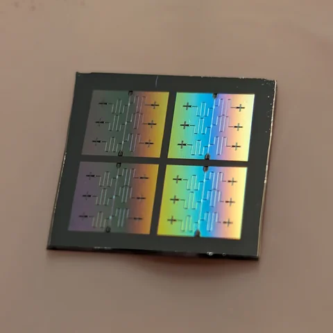 A patterned transmon chip before packagingOJB Quantum · CC BY 4.0
 Quantum System One at ThinkLabOnri Jay Benally (OJB Quantum) · CC BY 4.0
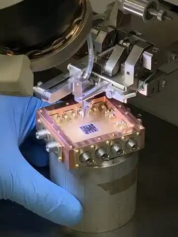 Inside an AQT processor packageAdvanced Quantum Testbed/Berkeley Lab · NQI gallery reuse permission
 Inside the SQMS Quantum GarageRyan Postel / Fermilab · NQI gallery reuse permission
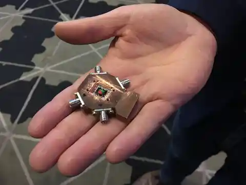 Three qubits in the palm of a handAnita Fors (Chalmers) · CC BY-SA 4.0
 Sycamore on displayColdupnorth · CC BY-SA 4.0
Back to all images · Explore the interactive Model · Image rights and corrections