
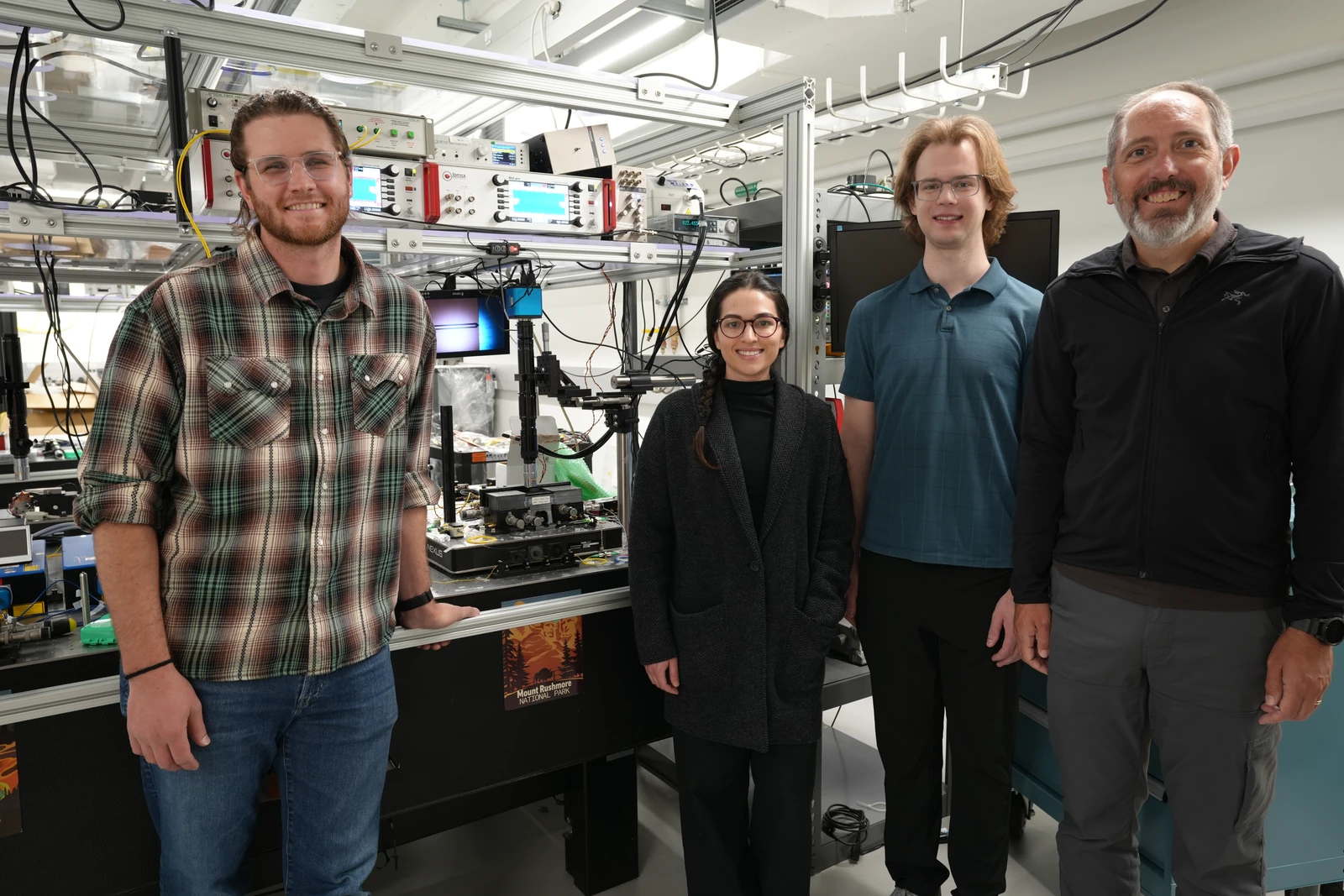
The NIST team behind the any-wavelength photonics chip
A chip photograph can hide the laboratory needed to develop and measure it. This wider view restores that context: researchers, racks, instruments and a crowded optical table surround a device whose dimensions are much smaller. The NIST source identifies the team associated with its integrated-photonics work. Use the photograph to introduce the collaboration, then let a device close-up explain scale. The phrase “any wavelength” needs a careful explanation of demonstrated tuning, conversion and material limits in the reporting. Nothing in a team portrait establishes an unlimited operating range or readiness for manufacture.
- Organization
- NIST
- Image type
- Photograph
- Capture date
- Not supplied by source
Source publication and upload dates are separate from capture dates. The capture date is not verified.
- Photographer / creator
- R. Jacobson/NIST
- Reuse terms
- Public domain in the United States; NIST worldwide reuse terms
R. Jacobson/NIST — The NIST team behind the any-wavelength photonics chip — Public domain in the United States; NIST worldwide reuse terms — https://www.nist.gov/image/members-nist-quantum-and-nonlinear-nanophotonics-group-any-wavelength-photonics-chip — https://www.nist.gov/open/copyright-fair-use-and-licensing-statements-srd-data-software-and-technical-series-publications.
Full original frame retained; EXIF orientation normalized where present, resized without enlargement and converted to WebP. No crop or content alteration.
Read the image
A small chip can have a large measurement environment
The wider laboratory view is a useful companion to a device close-up because it restores what the close-up leaves outside the frame. The team stands beside an optical table, instruments and cables. Those objects make it easier to ask how an output is generated, controlled and measured, without guessing the function of every component.
A reader may see a miniaturized chip and assume the entire experimental system has already been miniaturized. That conclusion does not follow. A small component can be developed or characterized using a larger laboratory environment. The photograph is an opportunity to separate the size of a device from the size of the system needed for a particular task.
Use the source-identified team and the associated chip as a two-part introduction. Let the wider image supply human and experimental context, and let the chip image supply scale. A claim about integration, manufacturing or wavelength coverage still needs its own evidence.
Can we identify each instrument’s job from the photograph?
Only when a visible label or the source supports that identification. A familiar-looking rack is not enough to infer its configuration or performance.
Does a crowded bench imply an immature technology?
No. Research and characterization setups serve different purposes from deployed products. The intended task and system boundary must be stated before making that comparison.
An independent QubitWire lesson based on this image and the cited source reading. The image does not establish a performance result.
Keep exploring
More from the same organization or hardware architecture.
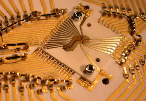 Gold electrodes for trapped ionsBlakestad/NIST · NQI gallery reuse permission
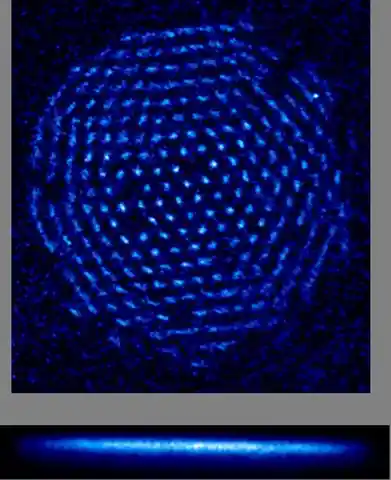 A crystal of trapped ionsNational Institute of Standards and Technology · Public domain (U.S. Government)
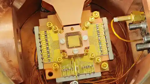 NIST’s beryllium-ion apparatusY. Colombe / NIST · Public domain (U.S. Government)
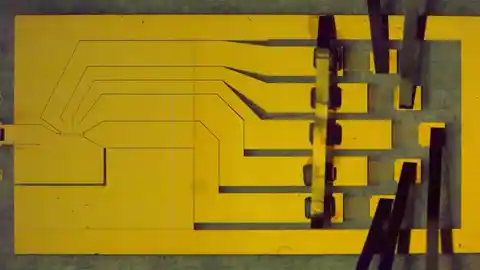 Gold electrodes for trapping ionsSigne Seidelin and John Chiaverini / NIST · Public domain (U.S. Government)
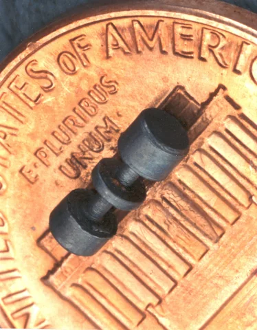 An ion trap resting on a pennyJ. Bergquist and D. Wineland / NIST · Public domain
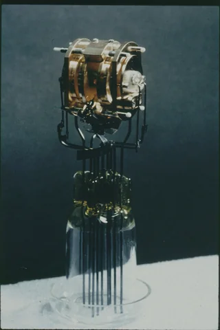 An early laser-cooling ion trapNIST · Public domain
Back to all images · Explore the interactive Model · Image rights and corrections