
Quantum in pictures
The connection that keeps a photonic chip useful
A chip held in tweezers puts an easily overlooked engineering problem in focus: getting light into a device, and keeping that connection reliable.
Research context: October 19, 2026 · Source review: October 20, 2026
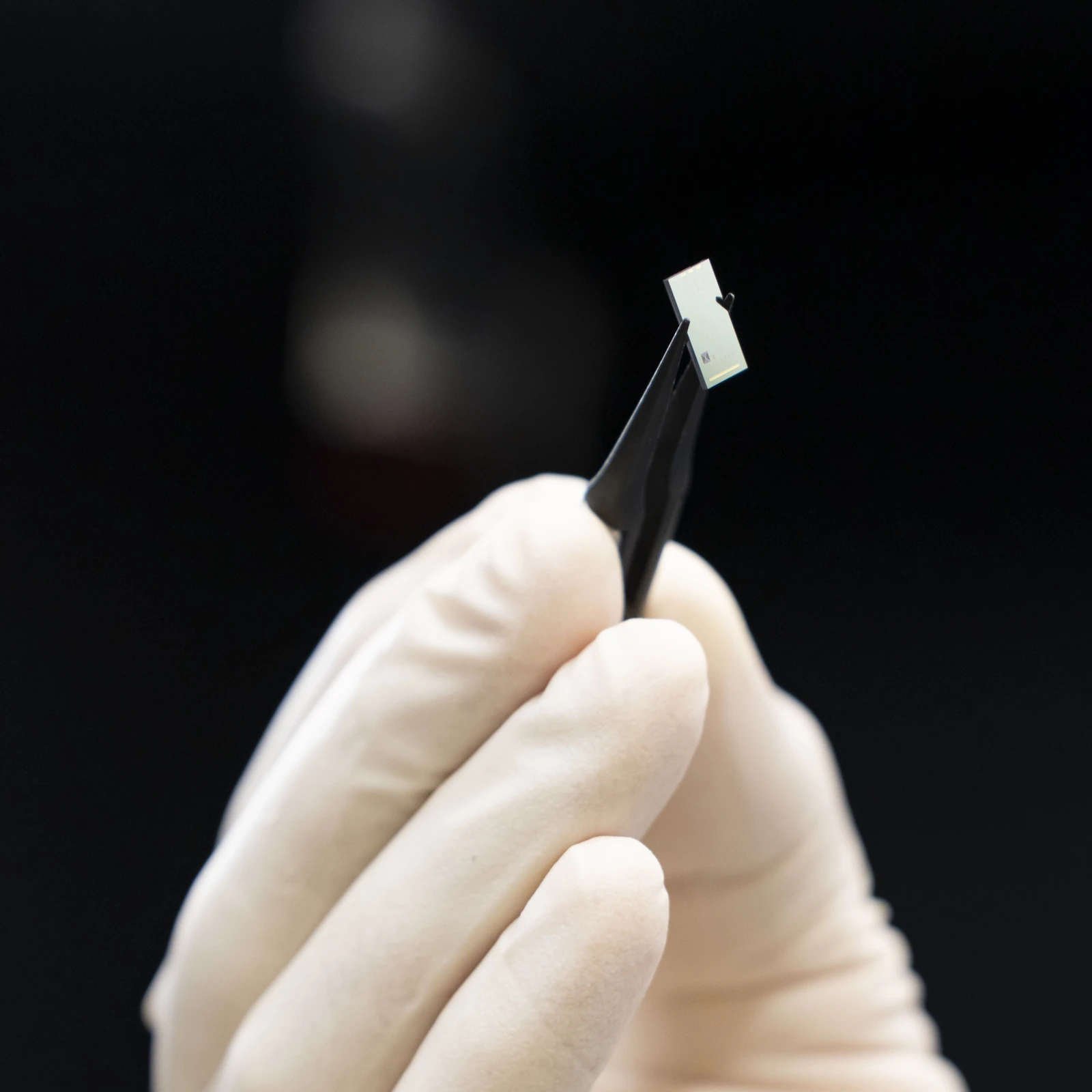
A rectangular chip and the tips of the tweezers are almost the only sharp objects in the frame. That simple composition makes this a practical lead image for a story about packaging, provided the caption names what it can establish. NIST supplied the photograph with reporting on connections designed for demanding environments. The image shows the object’s small physical scale; it does not show the bond chemistry or certify that every proposed environment has been tested. Keep the complete chip and tweezer tips in any crop. Use the accompanying article to explain tested conditions and distinguish them from future applications.
M. King/NIST — A photonic chip held in tweezers — Public domain in the United States; NIST worldwide reuse terms — https://www.nist.gov/news-events/news/2026/03/nist-researchers-develop-photonic-chip-packaging-can-withstand-extreme — https://www.nist.gov/open/copyright-fair-use-and-licensing-statements-srd-data-software-and-technical-series-publications.Full original frame retained; EXIF orientation normalized where present, resized without enlargement and converted to WebP. No crop or content alteration.
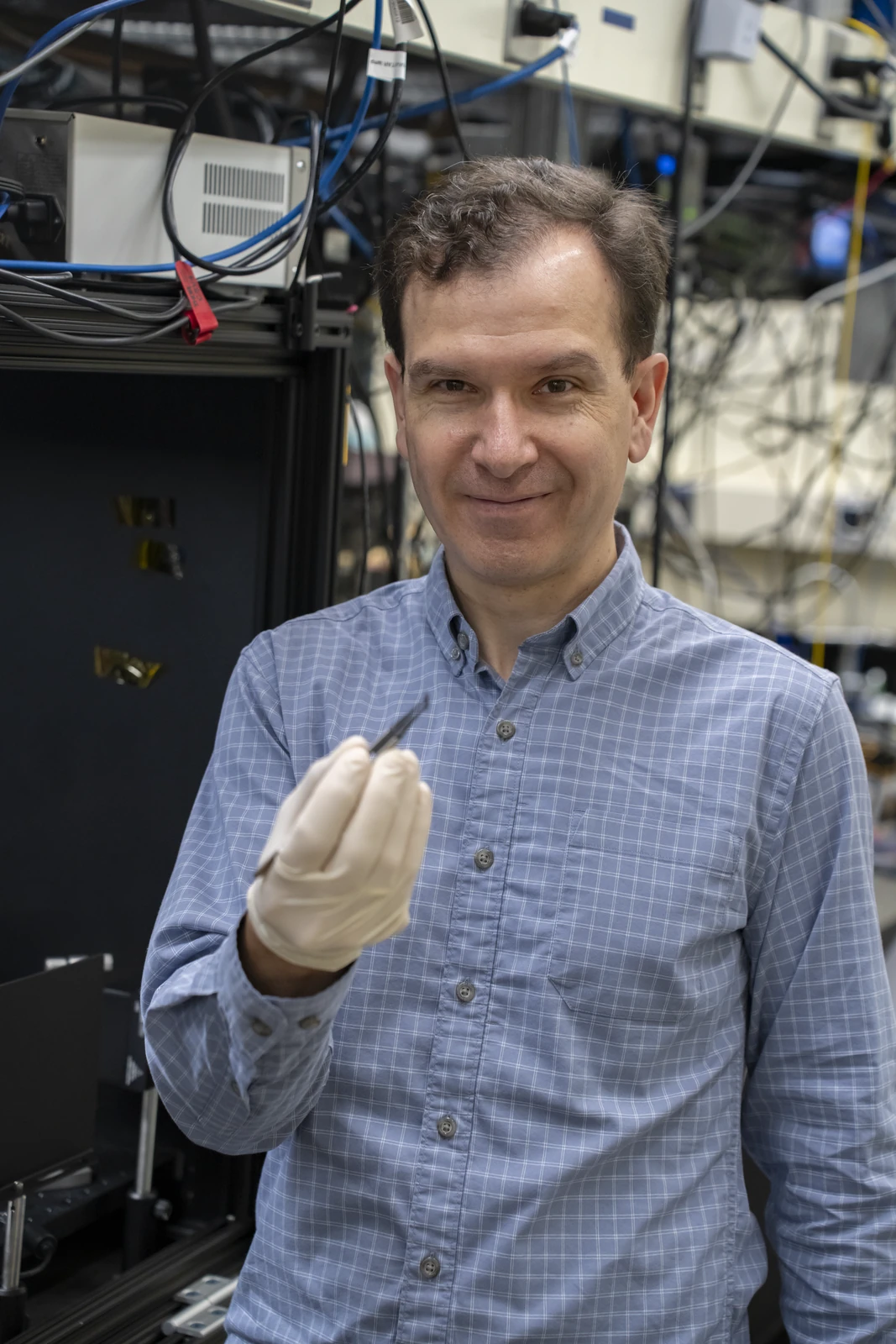
The white glove and tweezers give the chip a useful human scale. They also move attention toward a practical problem: a small optical component has to connect reliably to the rest of an instrument. NIST identifies the researcher as Nikolai Klimov and associates the photograph with work on packaging for harsh environments. The image does not reveal how the connection was made or how it survived testing. Pair this portrait with the closer chip photograph, then explain which claims come from laboratory tests. Keeping those roles separate allows a compelling human image to support a precise engineering story.
M. King/NIST — Nikolai Klimov holds a photonic integrated chip — Public domain in the United States; NIST worldwide reuse terms — https://www.nist.gov/image/nikolai-klimov-photonic-integrated-chip — https://www.nist.gov/open/copyright-fair-use-and-licensing-statements-srd-data-software-and-technical-series-publications.Full original frame retained; EXIF orientation normalized where present, resized without enlargement and converted to WebP. No crop or content alteration.
A pale rectangle sits at the tips of black tweezers. The gloved hand beneath it gives the object scale, while the blurred background removes almost every distraction. This is an unusually effective photograph for a story about a connection. The connection itself is too small to explain from the photograph; the object that depends on it is unmistakably physical. A wider companion image identifies the researcher, Nikolai Klimov, and returns the chip to its laboratory setting.[1][2]
The reporting context is a NIST packaging study published in March 2026. The researchers used hydroxide catalysis bonding to join optical fiber and chip with an inorganic connection. NIST reports tests involving cryogenic conditions, temperature swings, radiation and vacuum. It also gives a consequential qualification: high-temperature tests were not performed directly on the packaged chip because the available commercial fibers limited that experiment. Manufacturing speed remains a development issue.[3]
That qualification makes the story more useful. A reader considering a harsh-environment claim needs to know which object underwent which test. “The material survived,” “the connection remained aligned” and “the complete device kept operating” are different statements. Each may matter, but substituting one for another hides the boundary of the evidence. The test article, operating condition and measured response should remain together whenever the result is summarized.
Imagine preparing a comparison table for two hypothetical packages. One has an excellent measurement under a single difficult condition. The other has less dramatic performance but has completed a wider sequence of tests. Neither is automatically the better choice. A mission or instrument imposes its own sequence: storage, transport, installation, cooldown, operation and perhaps repeated maintenance. The relevant question is how the package behaves along that sequence, including changes that occur between measurements.
The photographs help readers understand why this matters without pretending to answer it. A chip is small, but an operating system has to reach it. Light arrives through a connection; the component sits in a mount; someone aligns, handles and checks the assembly. A useful visual feature can therefore follow the route from a person’s hand to a microscopic interface, then return to the larger instrument. The narrative gains scale at each step while the evidence remains attached to the appropriate claim.
For an editor, this creates a concrete interviewing agenda. Ask how alignment is measured before and after a test. Ask which failure would end the experiment and which change would merely degrade performance. Ask how many packages were tested and whether the reported examples capture the distribution. Ask what would have to change to make the process repeatable at the required production volume. These questions do not assume a failure; they establish what successful engineering would mean to the eventual user.
The close-up also rewards a restrained crop. Keep the whole chip and both tweezer tips visible, because they explain handling and scale. Use the wider portrait when introducing the researcher. Neither image should be labeled as a picture of the bonding reaction or environmental test. The publisher explicitly replaced an earlier AI illustration with real photographs, so the distinction is part of the asset’s provenance.[3]
The story’s payoff is the connection between a modest object and a demanding job. A promising chip becomes more useful when its interfaces are understood, measured and made repeatable. These photographs give readers a place to begin asking those questions.
Sources and further reading
- NIST packaging article and real replacement chip photograph ↗NIST
Specific image credit, tested conditions, high-temperature test boundary, process-development context and replacement-image note.
- Nikolai Klimov with photonic integrated chip ↗NIST
Researcher identity and M. King/NIST photo credit.
- Photonic Chip Packaging for Extreme Environments ↗NIST
Same primary page as source 1; duplicate citation marker does not create a second source budget.