
A Photonic Quantum Prototype Put Its Light Sources and Router on One Chip
A new preprint reports two tunable quantum-dot emitters, cryogenic routing and single-photon tests in one GaAs circuit. The integration matters more than the device count.
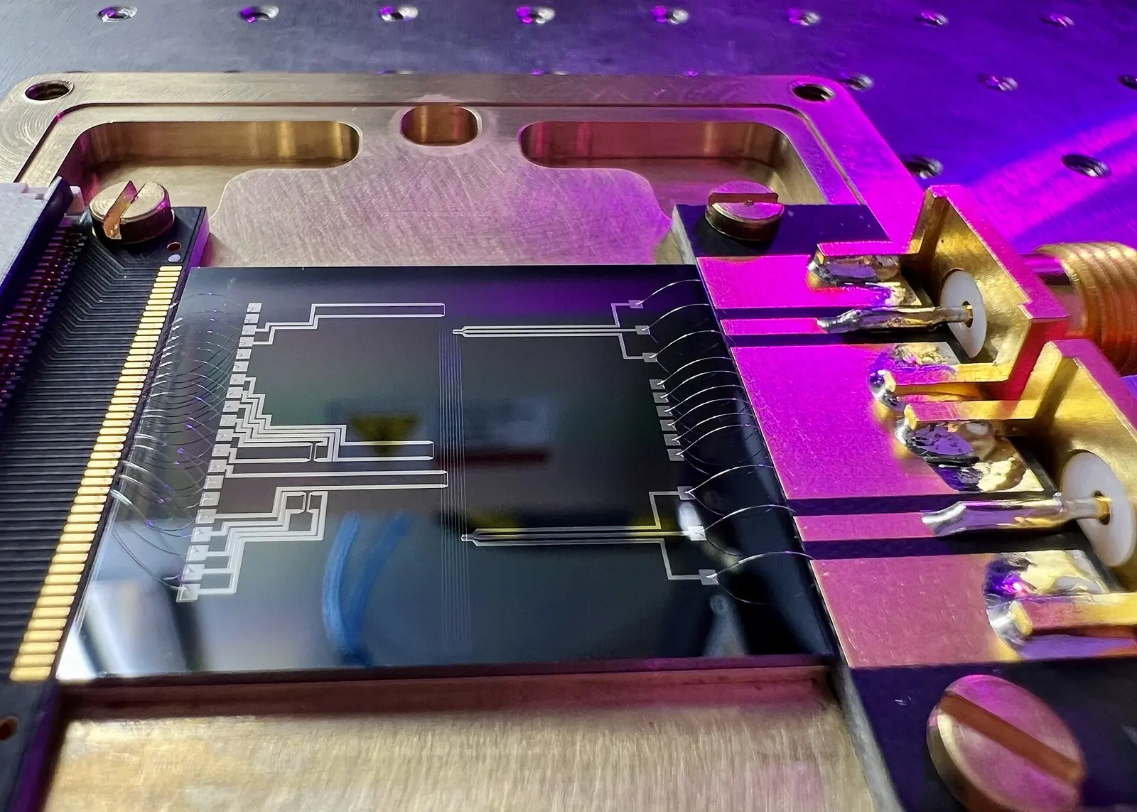

A preprint submitted October 5 reports a photonic quantum prototype that puts two independently tunable quantum-dot emitters, a reconfigurable nanomechanical router and their electrical controls on one gallium-arsenide circuit. That does not make a large photonic quantum computer. It shows that components usually demonstrated separately can operate together while the circuit still routes high-purity single photons.[1][2]
The hard part is coordinated control
The integration problem is partly electrical. The emitters operate near one volt while the nanomechanical router needs tens of volts, so the team isolated the router electrode and referenced it to the emitter diode's anode. Suspended waveguides then carry light between emitters, a tunable splitter and grating couplers. The useful step is coordinated control: the source and routing layers no longer have to be treated as separate laboratory demonstrations.[1][2]
The interference test used one source
The paper reports an average routed single-photon purity of g²(0) = 0.62% ± 0.07% across the router's tuning range. Its raw 62.2% ± 6.7% interference test did not compare the two integrated sources: it used consecutive photons from one quantum dot, with a fiber delay and final 50:50 beam splitter outside the chip. That test checks source indistinguishability in a partially integrated setup, not on-chip two-source interference.[2]
The earlier baseline was a two-source test
A 2023 paper from an overlapping team reported 79% ± 2% interference using two independently controlled emitters under continuous-wave excitation. That is a different experiment, not a record comparison. The new prototype adds programmable routing and common control but does not reproduce that prior two-source measurement on its new chip.[2][3]
Integration moves the bottleneck
QubitWire's analysis: photonic scaling will not be won by the best isolated emitter or switch alone. A useful architecture has to preserve quantum-light quality while sources, routing, voltage domains and packaging work at the same time. This prototype moves that systems boundary, but it also concentrates the next bottlenecks in wiring, optical coupling, fabrication yield and cryogenic packaging. Integration reduces one kind of laboratory handoff while making end-to-end engineering more visible.[1][2][3]
The next test needs a larger mesh
The main limitation is scale: the demonstrated paths are shorter than 100 micrometres and the paper does not show a many-emitter processor, fault-tolerant workload or end-to-end computational advantage. The informative next test is a larger mesh with many simultaneous emitters and routers that reports source-to-detector efficiency, crosstalk, control-line count, yield and interference stability across repeated cooldowns—not only the performance of selected devices.[1][2]