SkyWater opens OnRamp to help quantum startups plan their first foundry run
The practical terms behind a new route from laboratory design to a foundry.
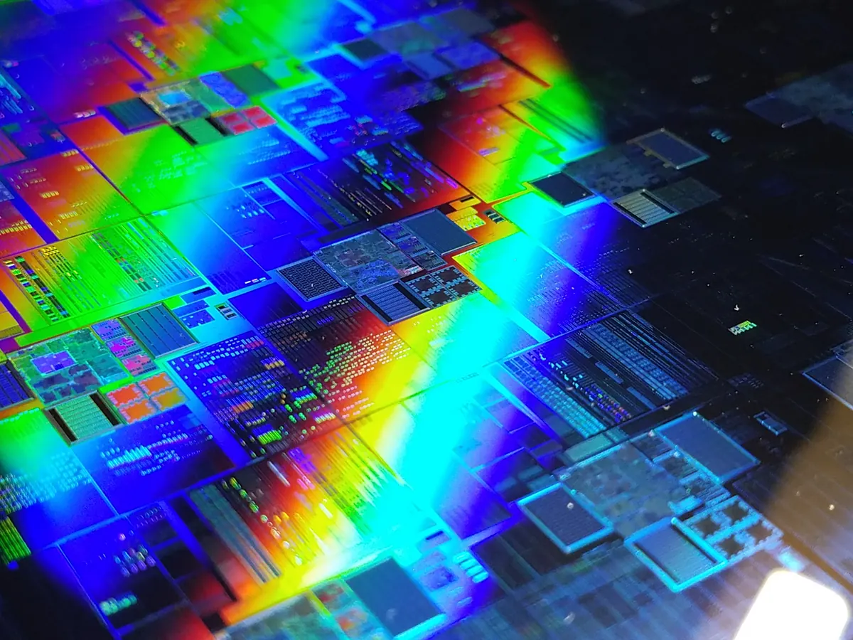

SkyWater has introduced OnRamp, a program intended to help early-stage quantum and photonics teams turn laboratory devices into a credible manufacturing plan. Selected companies can work with foundry engineers on materials, integration, packaging and the steps needed to fabricate their designs.[1][2]
The program centers on SkyWater's SP90 silicon-nitride photonics platform. Its published terms distinguish no-cost engineering work to scope a roadmap from access to prototype wafers, which is paid and depends on technical fit and availability.[1]
Editorial interpretation
That distinction matters for startups budgeting their first foundry engagement. OnRamp is an opportunity to clarify fabrication risks and milestones, not a blanket offer of free manufacturing.
For the quantum sector, the interesting question is whether earlier foundry involvement can make device plans more realistic. A manufacturable design needs more than an encouraging laboratory measurement. Teams must also account for process compatibility, packaging and repeatability. OnRamp gives founders a more concrete route to discussing those constraints before committing to a production path.
Learn: What a foundry-access offer actually buys
A foundry program can remove a costly uncertainty before it removes a manufacturing cost. Design review helps a team understand whether its proposed materials, device layout and packaging can fit an available fabrication process. That advice has value even when producing the wafers remains a separate paid activity.
SkyWater's OnRamp terms make this separation explicit: engineering work to scope a roadmap and access to prototype fabrication have different conditions. A reader assessing any similar offer should carry that distinction into the budget.[1]
Worked example
Hypothetical example: a startup expects to spend $20,000 on process planning, $45,000 on fabrication and $15,000 on packaging and initial testing. If a program covers the planning work, the remaining assumed budget is $60,000. Calling the entire project free would erase the two largest remaining commitments. These amounts illustrate the arithmetic and are not prices quoted by a foundry.
The next question is what the planning work produces. A useful deliverable might identify a compatible layer stack, unresolved material risks, the measurements needed after fabrication and a sequence of development runs. A vague promise of access is harder to evaluate than a written scope with responsibilities and milestones.
Selection conditions matter too. A program may accept only technically compatible projects or offer space on an existing development run. That can lower the barrier to a first device, while constraining timing or customization. A startup should understand whether those constraints fit its experiment before treating access as a committed production slot.
The practical value is reduced uncertainty: which decisions become easier, which costs remain and what evidence will show that the fabricated device performs reliably. The first wafer is a development milestone; repeatable performance and a sustainable manufacturing process require their own evidence.