
Xanadu’s GlobalFoundries Deal Targets Two Photonic Bottlenecks on a 300 mm Line
An October 6 manufacturing agreement targets low-loss optical circuits and photon-counting detectors. The next evidence should show whether the transferred process delivers repeatable components that meet a quantum system’s requirements.
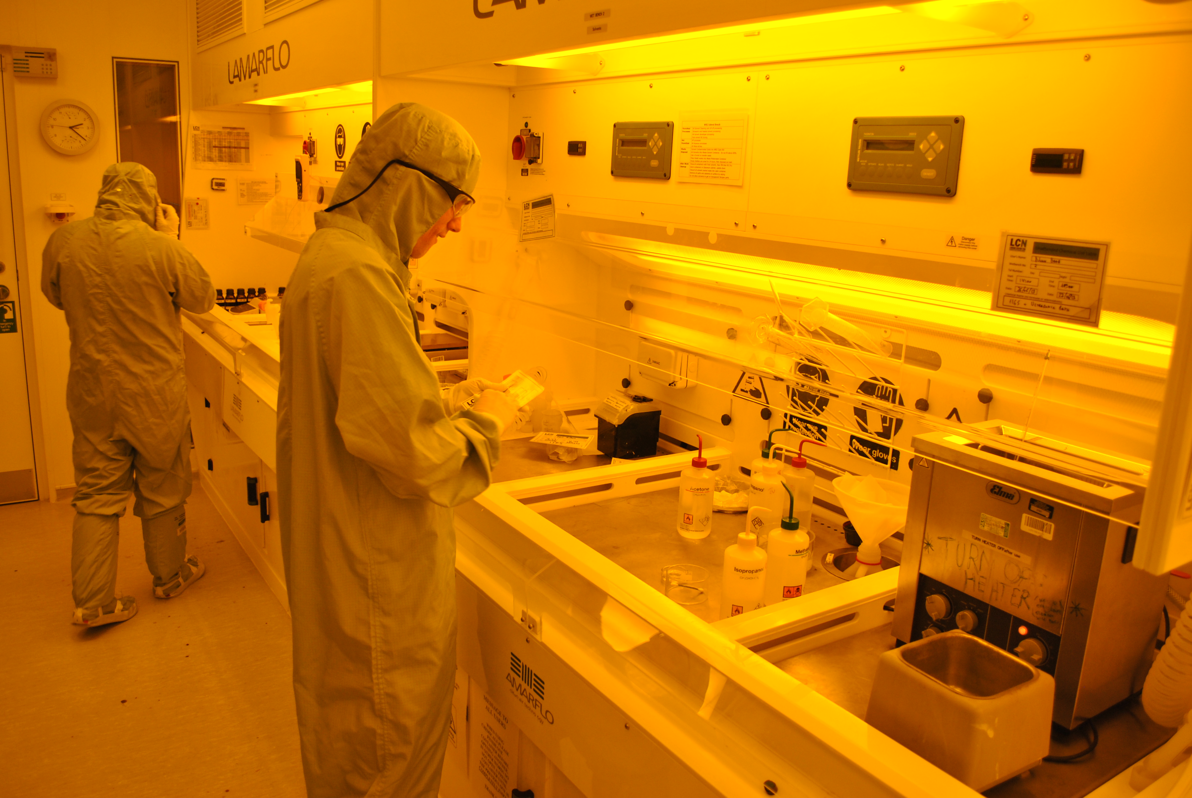

Xanadu is putting two critical photonic technologies on a commercial foundry roadmap. Its October 6 announcement names superconducting nanowire single-photon detectors and ultra-low-loss silicon-nitride photonics as the initial focus of a multi-year GlobalFoundries partnership. The target is GF’s 300 mm production line in Malta, New York. This is an industrialization agreement, with performance and volume-production outcomes still ahead.[1][5]
What changed since the earlier collaboration
There is an important historical baseline. Xanadu already announced a GlobalFoundries collaboration on March 7, 2022, centered on the GF Fotonix silicon-photonics platform and 300 mm fabrication. The new announcement therefore should not be described as their first partnership. Its specific news is the stated process-transfer focus on the detector platform and ultra-low-loss SiN technology.[1][2]
Two components, one system problem
The components address different parts of the same problem: keeping quantum light useful as a system grows. SiN circuits guide photons through optical hardware. Photon-number-resolving detectors distinguish how many photons arrive in a pulse, providing information needed by photonic protocols. Xanadu expects its chosen SNSPD platform to improve speed and reduce hardware overhead. Those benefits are company expectations, rather than measurements supplied by this agreement.[1][3]
The technical context comes from Aurora, Xanadu’s modular photonic system described in Nature in January 2025. That experiment connected 35 photonic chips and demonstrated primitive functions of the proposed architecture, including real-time decoding for a distance-two repetition code. The authors described it as a scale model operating below the performance needed for fault tolerance. They identified optical loss as the dominant obstacle to crossing the threshold.[3]
This explains why a manufacturing agreement can matter without announcing a larger working computer. The technical task is to preserve sufficiently good components while producing more of them. Increasing the number of fabricated devices will not rescue a system whose optical losses remain too high. The Aurora result establishes the relevance of that constraint; it does not validate the performance of a transferred GF process.[3][4]
GF’s Malta site supplies a concrete manufacturing setting. The company describes it as a large-scale, automated 300 mm facility supporting silicon photonics alongside several electronic semiconductor technologies. The wafer diameter describes the production format. It is not a measure of quantum accuracy, detector efficiency or logical computing performance. Those require their own tests on the devices emerging from the relevant process.[4]
The next benchmark should describe a batch
QubitWire’s analysis: the useful manufacturing comparison is a distribution, not a single exceptional device. Ask how consistently the transferred process meets an optical-loss budget and a detector-performance requirement across a fabricated batch. Then ask how many usable components survive packaging and connection into modules. A strong best-case result can coexist with poor repeatability; an industrial process becomes valuable when enough components meet the same system requirements.[1][3][4]
That proposed test is an engineering inference from the stated process transfer and Aurora’s loss constraint. It is not a reported yield result. The October release provides no transferred-process loss measurement, detector-efficiency distribution or production-yield figure. Its risk disclosure expressly identifies process transfer, yield, quality and technical performance as uncertainties. A signed manufacturing pathway therefore cannot be counted as demonstrated fault-tolerant operation or high-volume shipment.[1][3]
Keep the operating conditions attached
Room-temperature photonics also needs careful wording. Aurora’s paper describes room-temperature packaged optical modules while explicitly separating a photon-number-resolving detection system housed in a cryostat. Its demonstrated sensors were a different implementation from the SNSPD platform named in the new agreement. Readers should neither erase the detector’s cooling infrastructure nor treat the 2025 experiment as a test of the new process.[1][3]
What would turn the agreement into an engineering result
The next informative evidence would connect three records: component measurements across a fabricated batch, packaged-module behavior and the architecture’s stated performance requirements. Publish the losses, detector results, acceptance criteria and variations together. That would let another team judge whether manufacturing scale is preserving the properties that matter. QubitWire proposes this checklist; neither the agreement nor the prior Aurora study reports that complete validation.[1][3][4]
For now, the development is consequential because it gives two important components a named industrial partner and production destination. The useful question has become more concrete: what performance can this transfer reproduce, how consistently and after which integration steps? Following those measurements will tell readers much more than treating a wafer size or a partnership headline as a finished quantum capability.[1][3][4]
Read the deeper explanation · about 6 min
This estimate covers the explanation below, separate from the overview. Optional depth was added in this reading edition. The article keeps one canonical address and its original chronology. Source review: . The relevant source dates and limitations are recorded below.
Imagine building a camera that almost never misses the light you care about, rarely imagines light that is not there, recovers quickly enough for the next event and works reliably across a large manufactured array. Now imagine that the camera is not taking holiday photographs. It is part of a computer whose answer depends on exceptionally delicate optical events.
That is a useful way into the manufacturing partnership announced by Xanadu and GlobalFoundries on October 6. The companies describe work on superconducting nanowire single-photon detectors and low-loss silicon-nitride photonics for a 300 mm manufacturing platform. Their announcement is about industrializing essential components, not presenting a newly completed fault-tolerant quantum computer.[1]
The distinction makes the story more interesting, not less. Quantum computing will need systems that can be built repeatedly, serviced and evaluated as systems. A striking laboratory device and a dependable manufactured component are related achievements, but they are not the same achievement.
The moment light becomes a record
A detector provides a bridge between an optical event and an electrical record. In a superconducting nanowire detector, absorbed light can briefly disrupt superconductivity in a small region, producing a measurable pulse. The device requires a carefully maintained cold environment. NIST's explanation emphasizes that efficiency, speed, false counts and photon-number resolution are different demands rather than a single universal rating.[2]
Think of a very quiet doorbell. It must notice a genuine visitor without ringing whenever a branch moves. It must also become ready for the next visitor quickly enough. That analogy describes a measurement problem, not the microscopic physics: photons are not miniature people and the detector is not reading a label attached to each one.
The record matters because a computation needs more than a state evolving somewhere inside an apparatus. It needs a way to extract the information its procedure is designed to produce. A readout chain that loses useful events or introduces misleading ones changes the usefulness of the whole procedure. The prettiest optical path is not necessarily the one that produces the best answer.
Four questions hidden inside the word better
When someone says a detector is better, ask which property improved. Detection efficiency concerns how many relevant incoming events are successfully registered under stated conditions. False counts concern records that do not correspond to the intended signal. Recovery and timing concern when the device can respond again and how precisely an event is placed in time. Counting one photon and distinguishing the number in a pulse can also be different tasks.[2]
A comparison is meaningful only when the conditions match the proposed use. A device can be excellent for one wavelength or operating regime without being the best choice for another. A high-performing isolated sensor can also behave differently after packaging, routing and readout are added. Those are engineering questions, not reasons to dismiss the original device result.
For readers, the practical rule is simple: do not collapse a specification sheet into a winner label. Ask what a particular system needs, which measurements address those needs and what was included in the test. A manufacturer that reports the awkward details gives an evaluator more useful information than a headline containing only the largest percentage.
Why the factory is part of the experiment
A manufacturing process must deliver more than an exceptional sample. It must produce enough acceptable devices with sufficiently predictable behavior. This introduces questions about variation, testing, packaging and the cost of identifying failures. These are general engineering considerations; the partnership announcement does not supply a complete public yield or cost model.[1]
Suppose, as an explicitly invented example, two processes can each make an excellent detector. One produces consistent devices that can be tested before expensive assembly. The other requires extensive adjustment after assembly. Their best measured detectors might look similar, while the effort required to build a working system differs greatly. The example does not estimate either company's process. It shows why a factory cannot be judged solely by a champion device.
The 300 mm figure describes the manufacturing platform's wafer scale. It is not a qubit count, a logical-qubit count or a count of functioning computers. Translating wafer area into useful machines requires assumptions about layout, yield, packaging, interconnection and system design. None should be invented merely because a large industrial number makes an appealing headline.
The loss budget belongs to the whole route
A photon can encounter more than one opportunity to be lost between preparation and measurement. A system-level evaluation therefore needs to account for the route rather than quote the performance of its best component in isolation. The precise route and relevant losses depend on the architecture; a generic diagram is not a measured budget for Xanadu's machine.
A simple arithmetic example conveys the issue without pretending to simulate the hardware. If three independent stages each transmit 90 percent of the relevant events, the combined transmission is 72.9 percent, not 90 percent. That calculation assumes independent, multiplicative stages. It ignores correlations and many physical details, but it demonstrates why several individually respectable numbers need not add up to the expected whole.
This is also why low-loss photonics and detector manufacturing belong in the same industrial story. Improving one end of a chain while neglecting another can leave the useful outcome constrained elsewhere. An honest performance account will state the boundary around the measurement and explain which parts of the route are outside it.
Light does not remove every refrigerator
The phrase photonic computing can invite a misleading picture of a completely warm machine. Photons are attractive information carriers, but a photonic architecture may still rely on components that require demanding environmental support. Superconducting nanowire detectors are a clear example.[2]
QubitWire's superconducting-computer Model should help explain that boundary, not blur it. A refrigerator in one architecture is not automatically the same refrigerator, temperature stage or component arrangement used in another. A visitor can learn the general reason environmental control matters while being told that the pictured assembly is not a literal rendering of Xanadu's system.
This is a useful test for every attractive hardware image: what exactly does it depict, and what is the caption asking the reader to infer? A real photograph with an inaccurate architectural implication can be more misleading than a clearly bounded original schematic.
What would change the story
The meaningful follow-ups are process qualification, repeatability, integration and eventually measured system outcomes. A new announcement matters when it adds evidence about one of those steps. A second statement of the same partnership should not be presented as a second technical breakthrough.
Readers should also distinguish a manufacturing milestone from a commercial or computational one. A qualified process may be important before it generates material revenue. Revenue may grow before a general fault-tolerant machine is demonstrated. A quantum benchmark may improve without proving a profitable manufacturing model. Each development answers a different question.
The larger point is that a quantum computer is not made useful by its most photogenic component alone. It becomes useful when its sources, routes, measurements, controls and supporting systems cooperate reliably enough to produce a defensible result. Counting photons is one place where that cooperation becomes visible. That makes the detector worth following even when it does not look like the star of the show.
Evidence for this explanation
- Xanadu and GlobalFoundries announce manufacturing partnership
6 October 2026 issuer-distributed release. The original investor-relations page returned an access block; this is the issuer’s same release, not independent corroboration.
- NIST: superconducting nanowire single-photon detectors
General detector explanation updated 25 September 2026. It explains the mechanism and distinct performance properties; its device metrics are not Xanadu manufacturing results.
Keep your reading trail
Keep up with these topics
Choose the subjects you want to find again in Your Updates.
What would turn this agreement into an engineering result?
Can the transferred process repeatedly produce components with low enough optical loss for an integrated logical-computing experiment?
The manufacturing announcement leaves this question open. Follow the company to find published research updates; a follow does not promise a future result or an email alert.