
A photographic collection · 14 photographs
Inside quantum hardware
Fourteen documentary photographs connect chips, cooling, optical equipment and atomic clocks with the systems around them. Each image keeps its original date, source and credit.
Published 24 October 2026 · Photographs from 2004–2025
An image records what was in front of the camera. It does not, on its own, demonstrate computing performance or identify the apparatus in a later news report.
Chapter 01
Chips and cooling
Start with the contrast in scale: a packaged processor can fit in a hand, while the apparatus around a processor occupies much more space. These photographs show different machines and architectures.
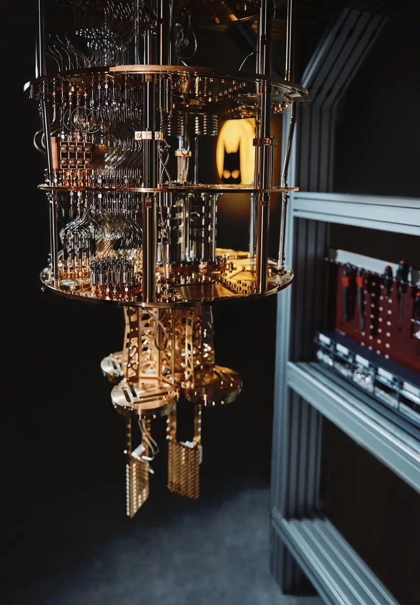
At the heart of Alice & Bob
The exposed Alice & Bob cryostat makes its layered construction and fine wiring visible. This is a laboratory photograph from 2024.
“Alice and Bob Cryostat” — Nilhope · CC BY-SA 4.0
Photographed 2024 · Archival image
Full original composition retained. Proportionally resized and converted to WebP; no crop, retouching or generated elements. These renditions remain under CC BY-SA 4.0.
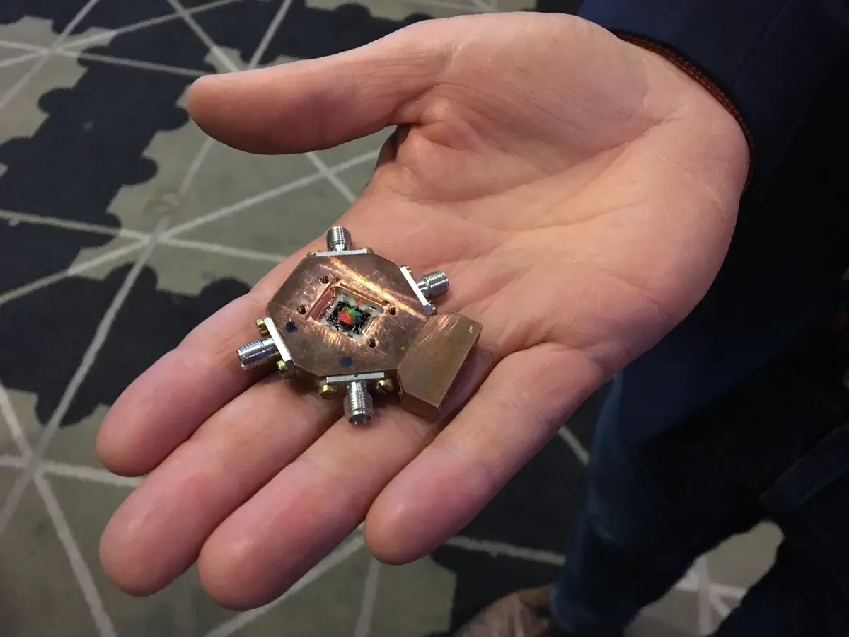
Three qubits in the palm of a hand
A hand provides scale for Chalmers’ packaged three-qubit processor. The visible package is only part of the experimental setup.
“Quantum-computer-Chalmers 2017” — Anita Fors (Chalmers) · CC BY-SA 4.0
Photographed 23 October 2017 · Archival image
Full available source composition retained. Proportionally resized and converted to WebP; no retouching or generated elements. These renditions remain under CC BY-SA 4.0.
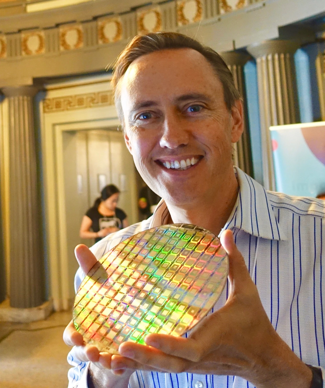
A wafer at human scale
A wafer provides a different view of fabrication: repeated patterns across a circular surface. This archival D-Wave image does not show the performance of a present-day machine.
Steve Jurvetson from Menlo Park, USA — The Beauty of Quantum Computers (25215168907).jpg — CC BY 2.0 — https://commons.wikimedia.org/wiki/File:The_Beauty_of_Quantum_Computers_(25215168907).jpg — https://creativecommons.org/licenses/by/2.0.
Photographed 1 February 2018 · Archival image
Full original frame retained; EXIF orientation normalized where present, resized without enlargement and converted to WebP. No crop or content alteration.
Chapter 02
Ions and communications
A close view of an ion-trap assembly and two views of quantum-key-distribution apparatus reveal different kinds of laboratory infrastructure. They come from separate NIST projects and years.
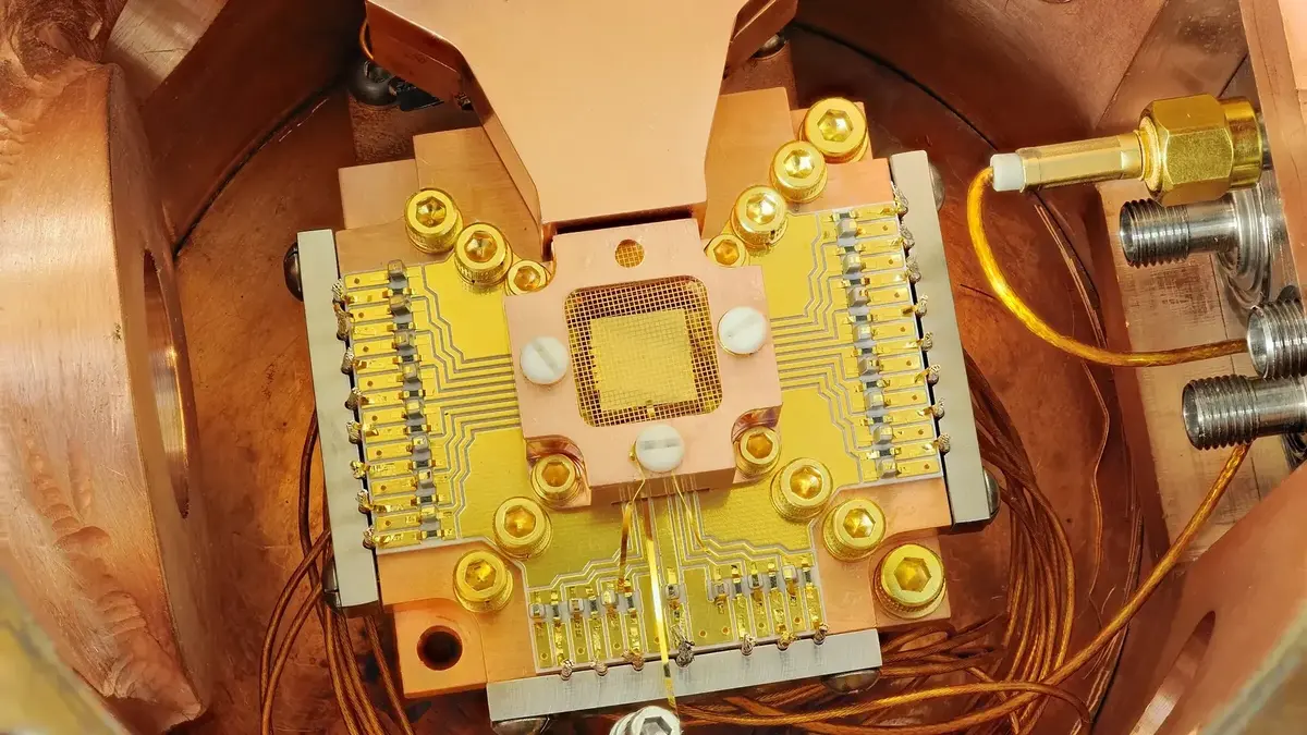
NIST’s beryllium-ion apparatus
The central opening, boards and connections belong to NIST’s historical beryllium-ion apparatus. This photograph does not depict a newly reported trapped-ion experiment.
“Quantum Computing; Ion Trapping (5941055642)” — Y. Colombe / NIST · Public domain (U.S. Government)
Photographed 23 February 2011 · Archival image
Prior QubitWire crop retained. Proportionally resized and converted to WebP; no retouching or generated elements.
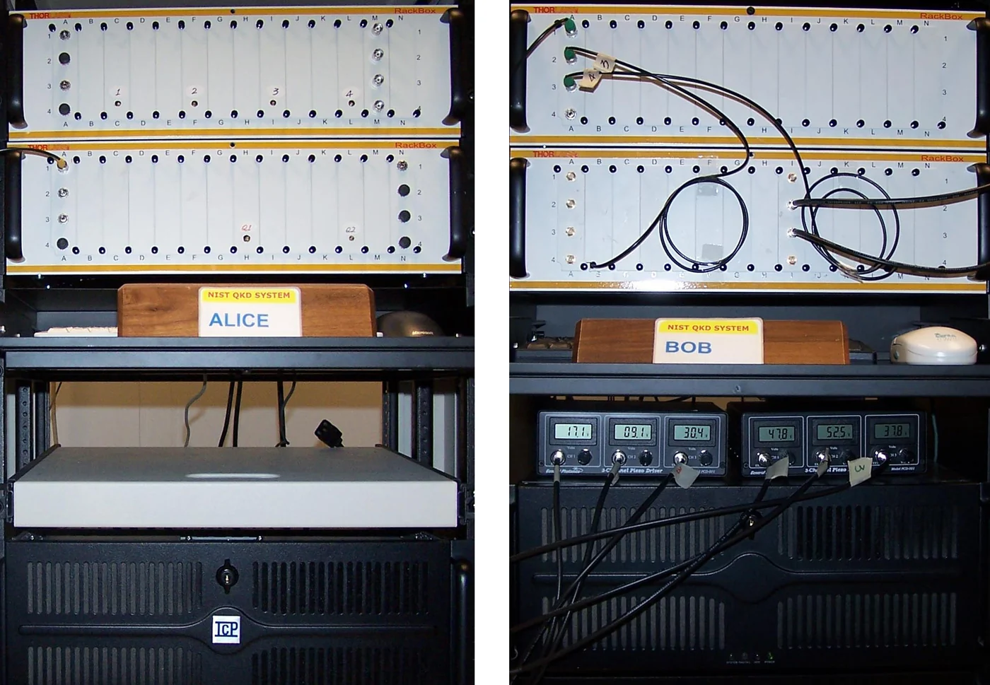
NIST’s fiber quantum-key-distribution racks
The labels Alice and Bob distinguish the two racks. Patch panels, cabling and instruments make the surrounding communications equipment visible.
NIST · US federal public domain
Photographed 27 September 2007 · Archival image
Full source composition retained. Proportionally resized and converted to WebP; no crop, retouching or generated elements.
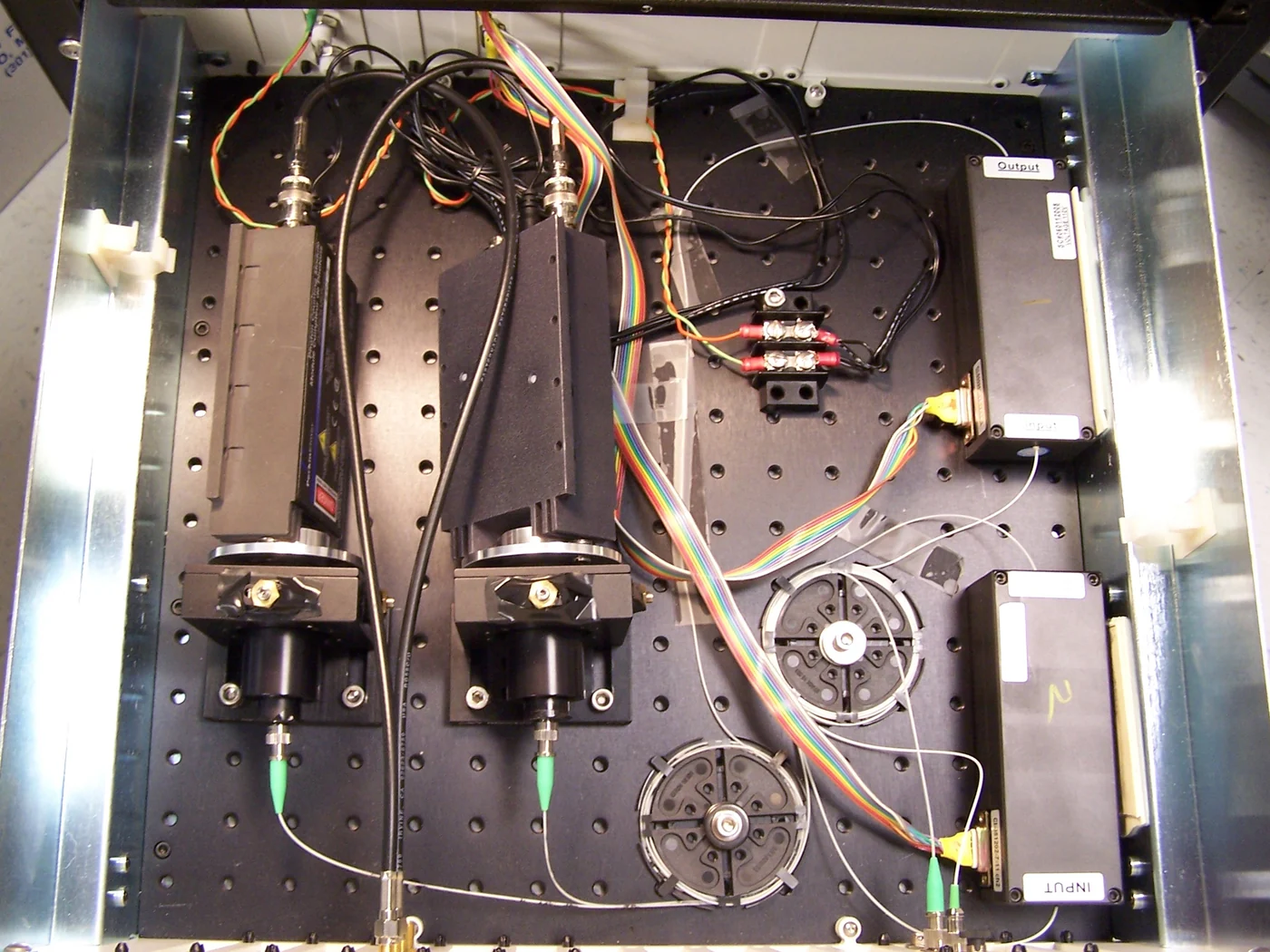
Inside a NIST quantum-key-distribution detector
An open enclosure exposes optical components and wiring in an earlier NIST detection setup. It is a separate photograph from 2004, not a close-up of the 2007 racks.
NIST · US federal public domain
Photographed 3 February 2004 · Archival image
Full source composition retained. Proportionally resized and converted to WebP; no crop, retouching or generated elements.
Chapter 03
Clocks and precision measurement
These archival NIST photographs move between a complete optical setup, miniature assemblies and the people at the laboratory bench. The different dates matter: they are not one continuous experiment.
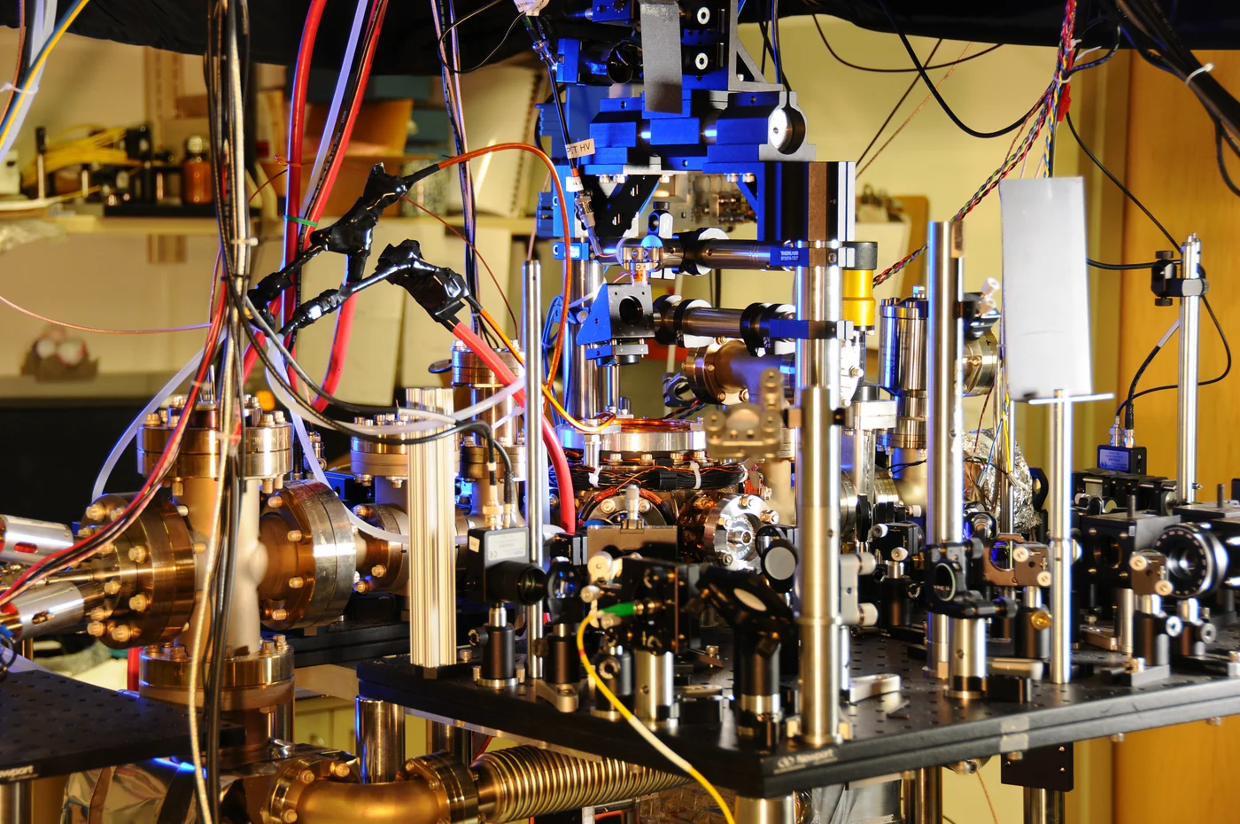
NIST ytterbium-clock apparatus
Metal mounts, optical components and cables surround the ytterbium-clock apparatus in this 2013 photograph.
Burrus / NIST · US federal public domain
Photographed 3 July 2013 · Archival image
Full source composition retained. Proportionally resized and converted to WebP; no crop, retouching or generated elements.
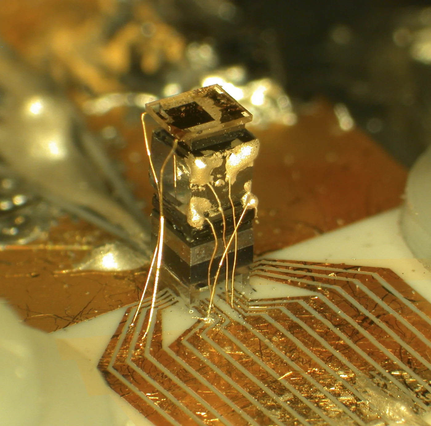
A miniature atomic-clock package
Fine connections rise from the patterned surface around a miniature clock assembly. This is a close view of physical equipment, not a diagram.
NIST · US federal public domain
Photographed 27 August 2004 · Archival image
Full source composition retained. Proportionally resized and converted to WebP; no crop, retouching or generated elements.
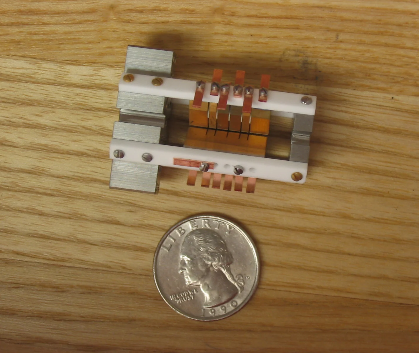
An aluminum-ion clock trap, with a coin for scale
A US quarter gives a familiar scale reference beside the aluminum-ion clock trap. The photograph dates to 2005.
J. Koelemeij / NIST · US federal public domain
Photographed 1 June 2005 · Archival image
Full source composition retained. Proportionally resized and converted to WebP; no crop, retouching or generated elements.
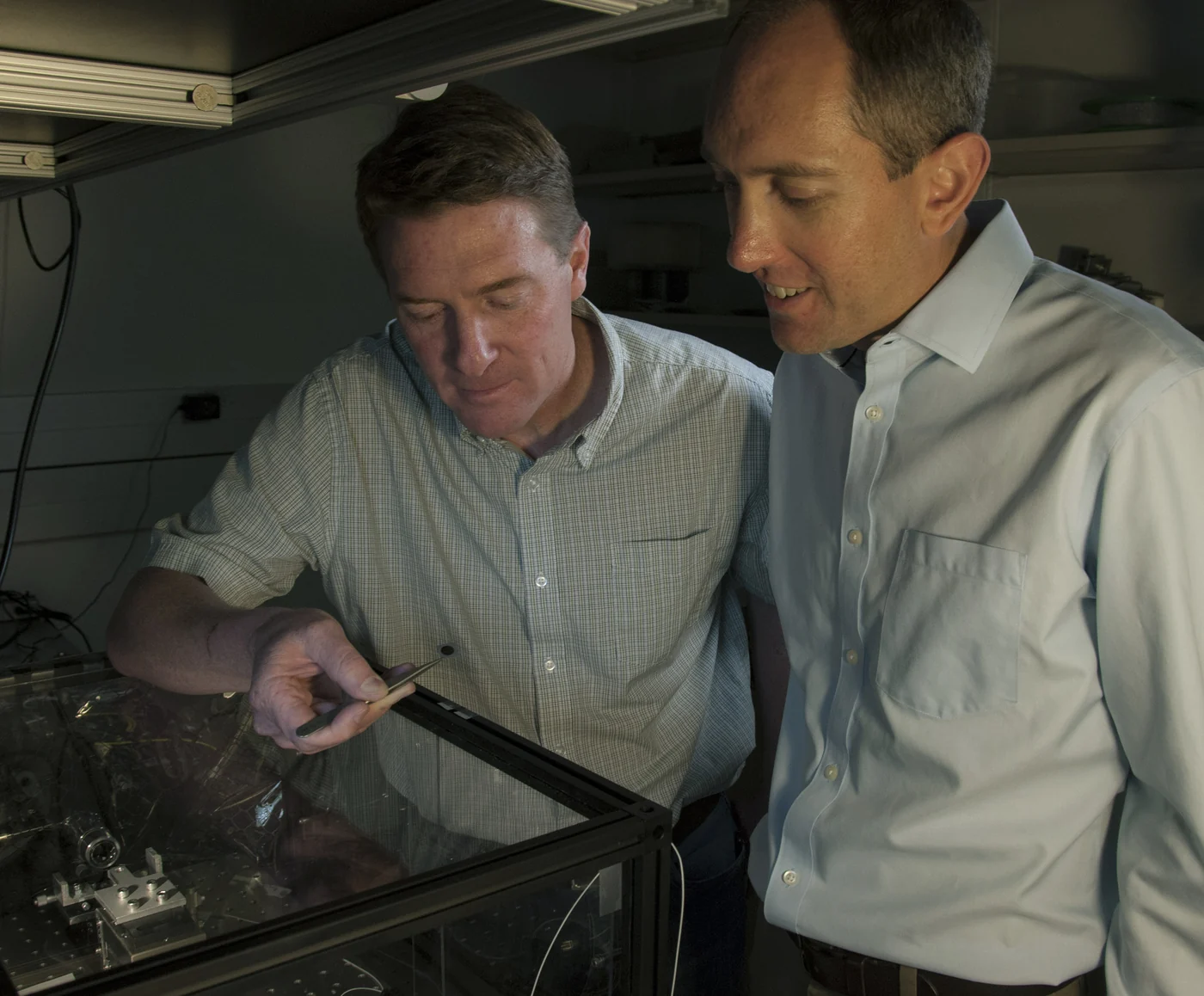
Frequency-comb research at NIST
Scott Diddams and Scott Papp inspect equipment at an optical bench. The people and the surrounding apparatus share the frame.
Burrus / NIST · US federal public domain
Photographed 18 June 2014 · Archival image
Full source composition retained. Proportionally resized and converted to WebP; no crop, retouching or generated elements.
Chapter 04
Systems and public displays
Three views document the 2025 inauguration of IBM Quantum System Two at Ikerbasque. A separate exhibition photograph shows demonstration hardware in Delhi in 2024. An inauguration, an operating installation and a demonstration display should not be confused.
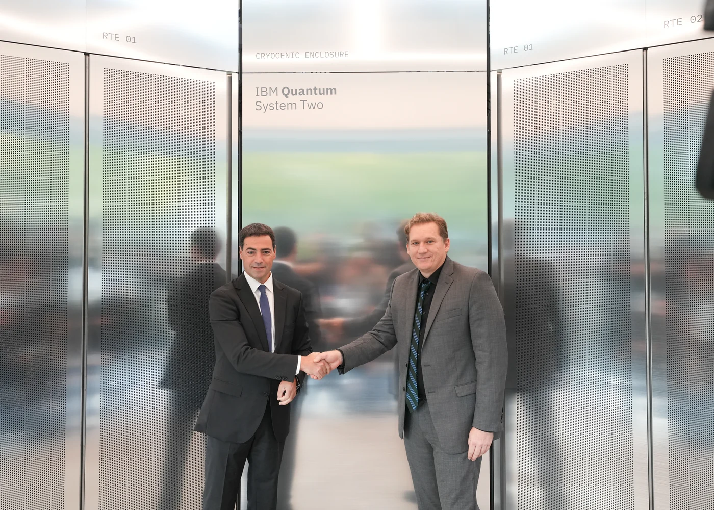
IBM System Two at its Ikerbasque inauguration
Imanol Pradales and Jay Gambetta shake hands beside the reflective IBM enclosure at the October 2025 inauguration.
Íñigo Sierra / Irekia–Eusko Jaurlaritza · CC BY 4.0
Photographed 14 October 2025 · Archival image
Full source composition retained. Proportionally resized and converted to WebP; no crop, retouching or generated elements.
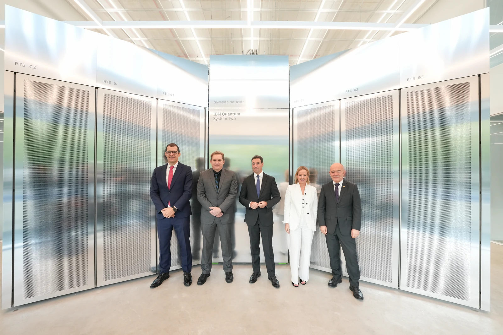
People beside Ikerbasque’s System Two
A wider group view shows the people and reflective enclosure at the same Ikerbasque event.
Irekia / Eusko Jaurlaritza — IBM Q System Two Ikerbasque 02.jpg — CC BY 4.0 — https://commons.wikimedia.org/wiki/File:IBM_Q_System_Two_Ikerbasque_02.jpg — https://creativecommons.org/licenses/by/4.0.
Photographed 14 October 2025 · Archival image
Full original frame retained; EXIF orientation normalized where present, resized without enlargement and converted to WebP. No crop or content alteration.
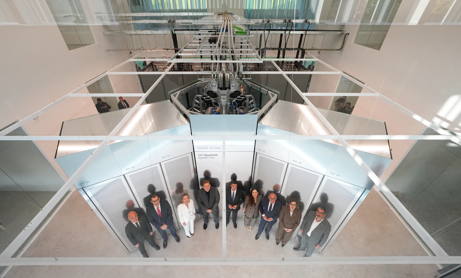
Looking down into the Ikerbasque installation
An overhead angle shows the shape of the enclosure and the group below. It is another view of the same 2025 event.
Irekia / Eusko Jaurlaritza — IBM Q System Two Ikerbasque 03.jpg — CC BY 4.0 — https://commons.wikimedia.org/wiki/File:IBM_Q_System_Two_Ikerbasque_03.jpg — https://creativecommons.org/licenses/by/4.0.
Photographed 14 October 2025 · Archival image
Full original frame retained; EXIF orientation normalized where present, resized without enlargement and converted to WebP. No crop or content alteration.
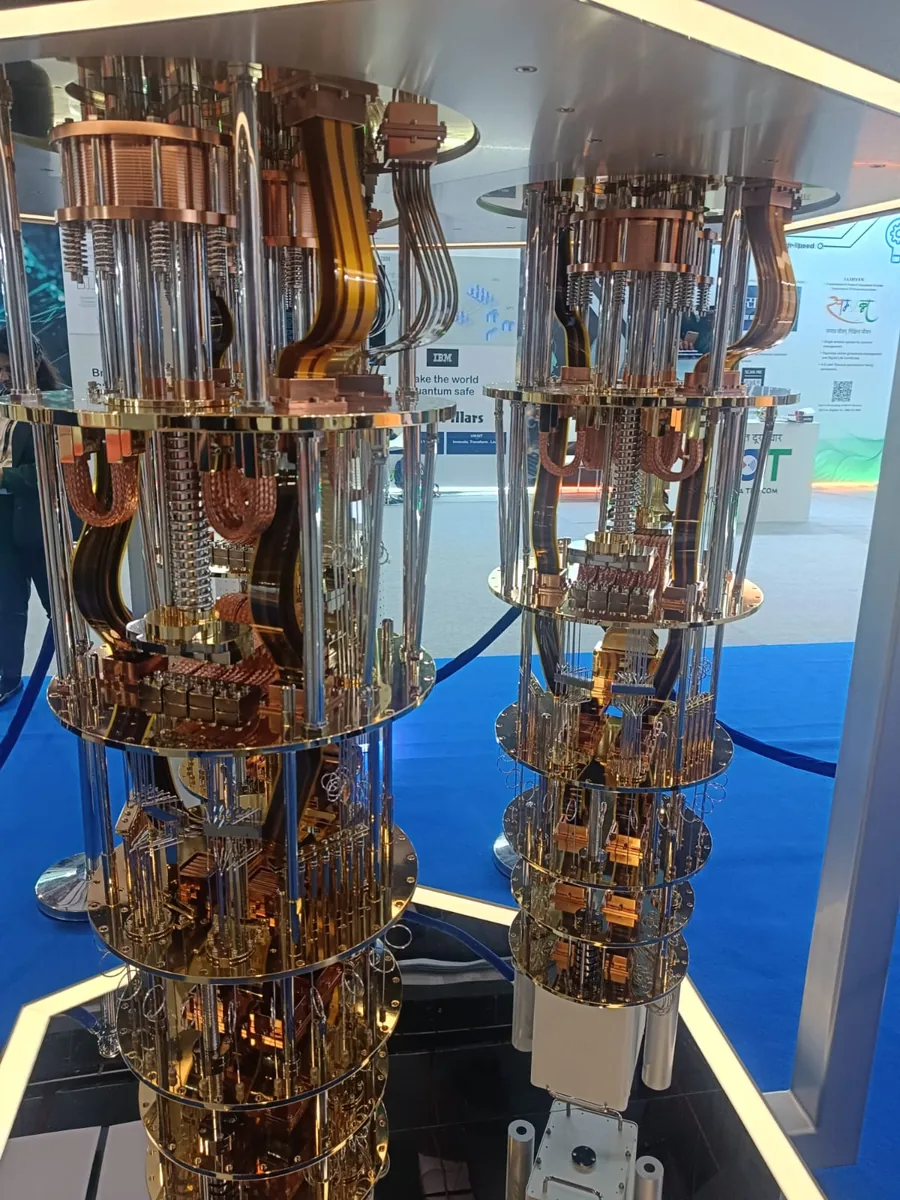
An IBM quantum-computer exhibition display
Two exposed demonstration assemblies at the 2024 WTSA exhibition in New Delhi. This display photograph does not establish that an operational quantum computer was running at the exhibition.
Dev Jadiya · CC BY-SA 4.0
Photographed 15 October 2024 · Archival image
Full source frame preserved. Resized proportionally and converted to WebP; no retouching, object changes or generated content. Image renditions retain the source CC BY-SA 4.0 license.