
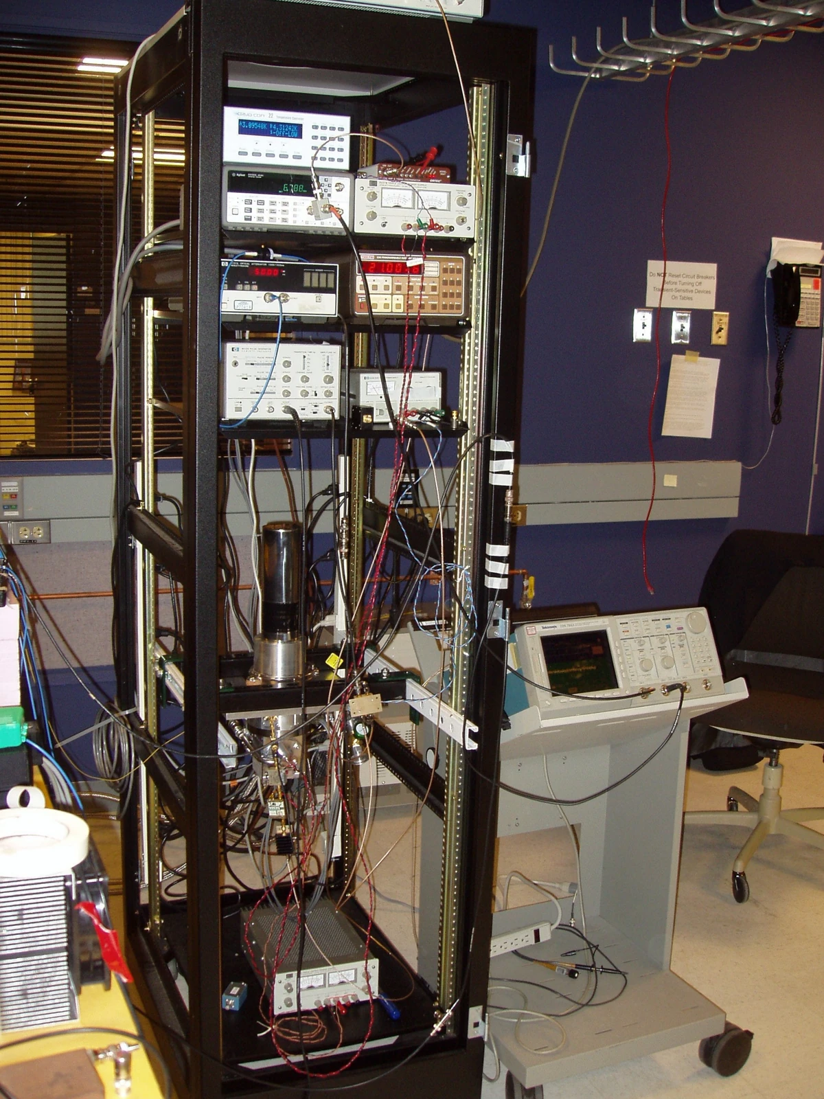
The instrument stack around a photon detector
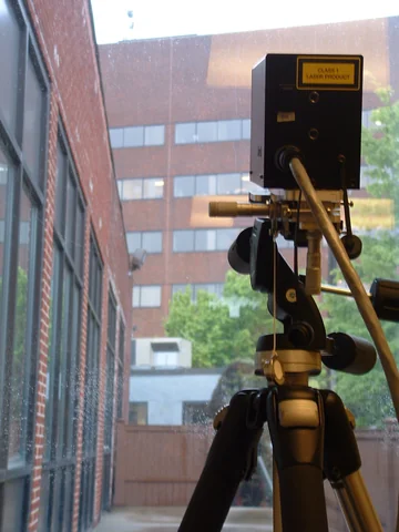
A detector can be a tiny sensing element and still rely on a substantial instrument stack. This photograph supplies that wider view. Its source identifies a superconducting-nanowire single-photon-detector setup in the DARPA Quantum Network and names the collaborating institutions. Use it alongside the smaller instrument photograph to ask which functions are performed by the sensing element and which belong to cooling, control, readout or recording. Those are teaching categories, not verified labels for each visible box. Keep the June 2005 date prominent so an early laboratory setup does not become an inaccurate illustration of a modern packaged product.
- Organization
- DARPA Quantum Network / BBN
- Image type
- Photograph
- Capture date
- 2005-06-16
- Photographer / creator
- Daderot
- Reuse terms
- CC0
Daderot — Superconducting nanowire single-photon detector in the DARPA Quantum Network (BBN) - June 2005 - P1010035.jpg — CC0 — https://commons.wikimedia.org/wiki/File:Superconducting_nanowire_single-photon_detector_in_the_DARPA_Quantum_Network_(BBN)_-_June_2005_-_P1010035.jpg — http://creativecommons.org/publicdomain/zero/1.0/deed.en.
Full original frame retained; EXIF orientation normalized where present, resized without enlargement and converted to WebP. No crop or content alteration.
Read the image
A nanowire detector has an instrument stack around it
An open rack contains instruments, cables and a cylindrical component beside more laboratory equipment. The source identifies a superconducting-nanowire single-photon-detector setup at BBN in June 2005, documenting collaboration among NIST, the University of Rochester and BBN.
The word nanowire describes a small sensing structure, while the photograph shows the system required to operate and read it. A detector needs an appropriate environment, electrical conditions and a way to turn a physical response into a usable signal. Those supporting functions can occupy far more space than the sensitive element itself.
This makes the image a useful counterpart to a device micrograph. A micrograph can explain local geometry; a rack photograph can explain integration. Neither alone establishes the complete detection efficiency, unwanted-event rate or timing behavior. A reader should follow the physical hierarchy from sensor to instrument to experiment, with a separate measurement source for performance.
Is the nanowire itself visible at this scale?
The photograph does not resolve the sensing structure. It documents the larger detector setup identified by the source.
Why can a tiny detector require substantial equipment?
Its environment, biasing, readout and data handling can need supporting hardware. The exact functions of pictured boxes require documentation.
What does the collaboration credit establish?
It records the source’s attribution of the setup. It does not imply current endorsement or that the same apparatus remains in operation.
An independent QubitWire lesson based on this image and the cited source reading. The image does not establish a performance result.
Keep exploring
More from the same organization or hardware architecture.
 The optical bench of an early quantum-network link
 An optical switch in a quantum-network experiment
 An early single-photon detector instrument
 A free-space endpoint facing another building
Back to all images · Explore the interactive Model · Image rights and corrections