
A photographic collection · 14 images
People and instruments
Fourteen documentary images connect researchers, laboratories, detectors and the equipment around a quantum experiment. Sources, image credits and date qualifications stay beside each photograph.
Published 27 October 2026 · Documentary photographs and a labeled micrograph, with source contexts from 2008–2026
The captions distinguish known camera dates from report and upload dates. A photograph records an apparatus, people or a place; computing performance needs separate evidence.
Chapter 01
The people and the places
A portrait records a person. A team photograph records a group at a moment in time. Buildings provide institutional context. Each tells a different part of the story around research.
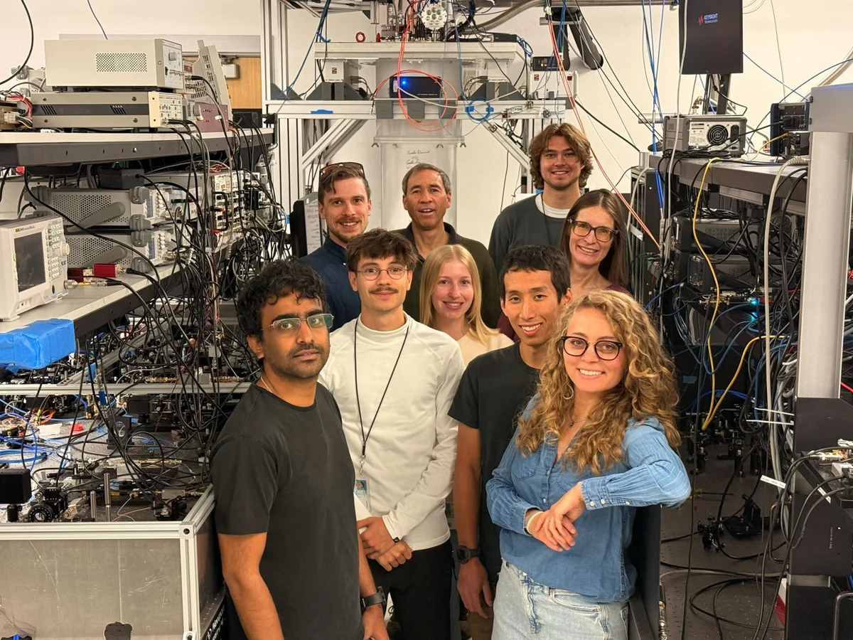
2026 Quantum Networking and Transduction Team
NIST’s Quantum Networking and Transduction Team stands among racks and optical equipment. The source uploaded this photograph in August 2026; the camera date is not established.
NIST · NIST public information reuse terms
Capture date not established · Archival photograph
Proportional resizing and WebP re-encoding. No crop, compositing, recoloring or content removal. Original source and license retained.
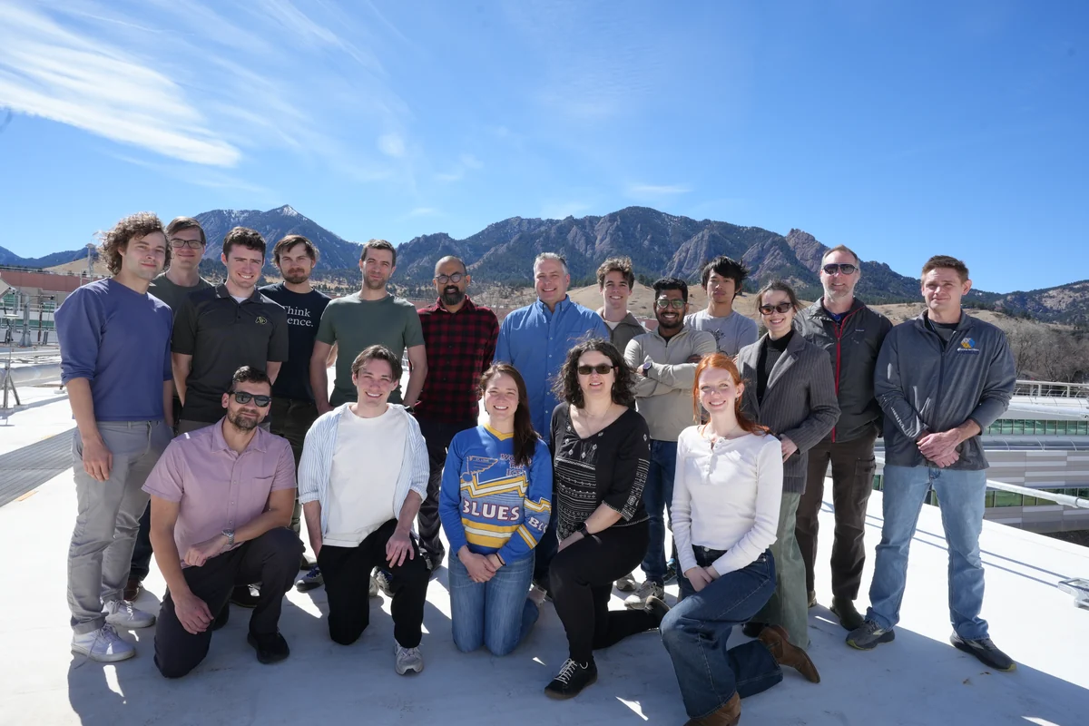
AMP group - March 2026
The Advanced Microwave Photonics group poses outdoors in March 2026. NIST’s caption dates the group photograph, making it distinct from the later upload date.
NIST · NIST public information reuse terms
Photographed March 2026 · Archival photograph
Proportional resizing and WebP re-encoding. No crop, compositing, recoloring or content removal. Original source and license retained.
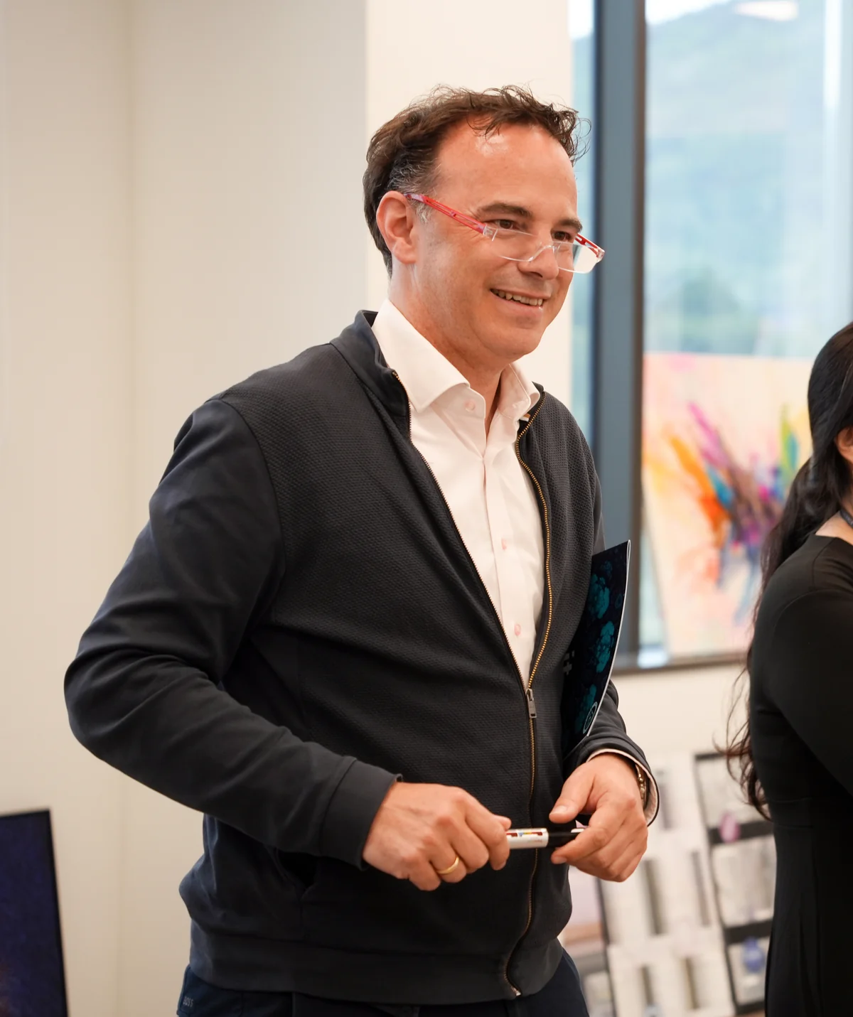
Markus Aspelmeyer (quantum physicist) front photo
Markus Aspelmeyer visits the Center for Quantum Nanoscience in Seoul in May 2024. A portrait provides human context; the research claims remain with their separately cited papers.
Rickinasia · CC0 1.0
Photographed 7 May 2024 · Archival photograph
Proportional resizing and WebP re-encoding. No crop, compositing, recoloring or content removal. Original source and license retained.
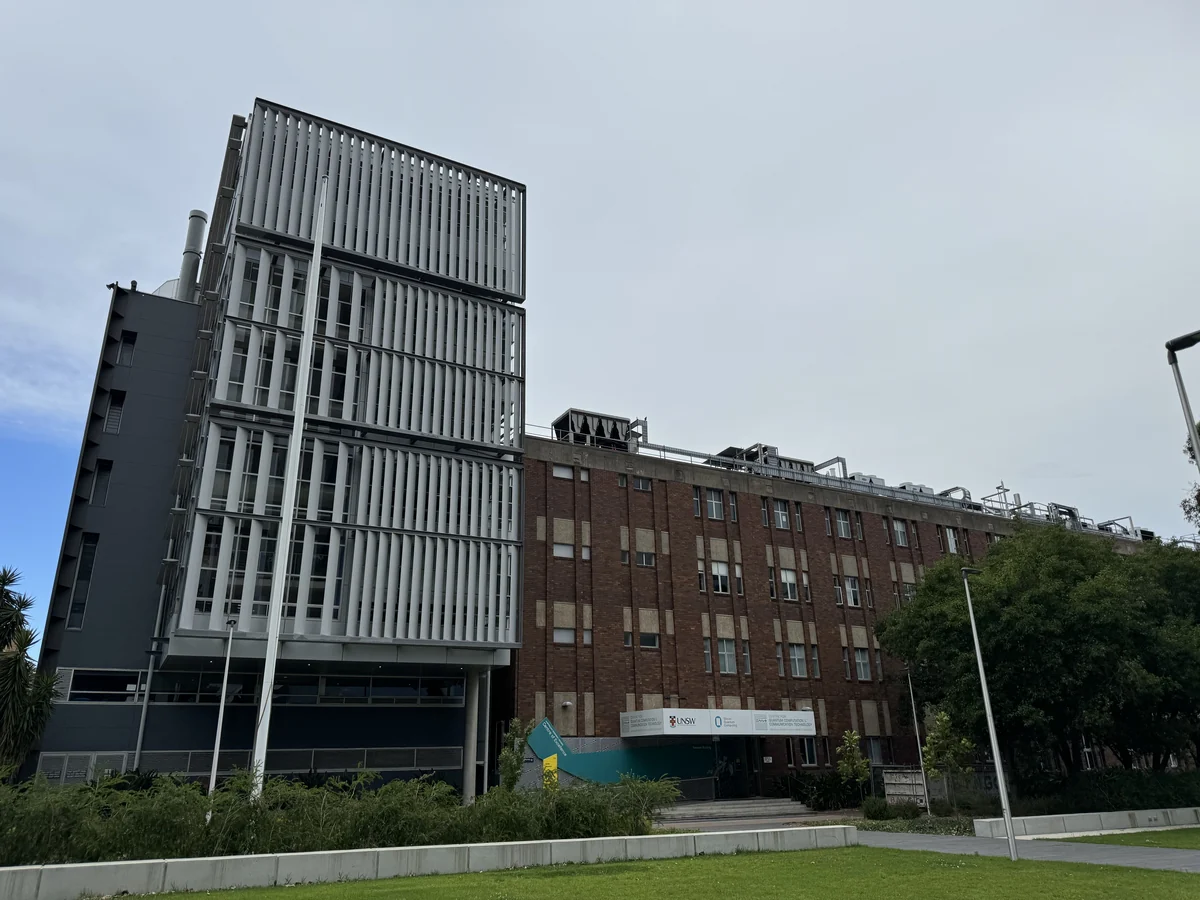
UNSW Newton Building and ARC Centre of Excellence for Quantum Computation and Communication Technology
The Newton Building and quantum-computation centre at UNSW, photographed in January 2025. The exterior supplies location context for research inside the institution.
FlyingKoala · CC BY 4.0
Photographed 5 January 2025 · Archival photograph
Proportional resizing and WebP re-encoding. No crop, compositing, recoloring or content removal. Original source and license retained.
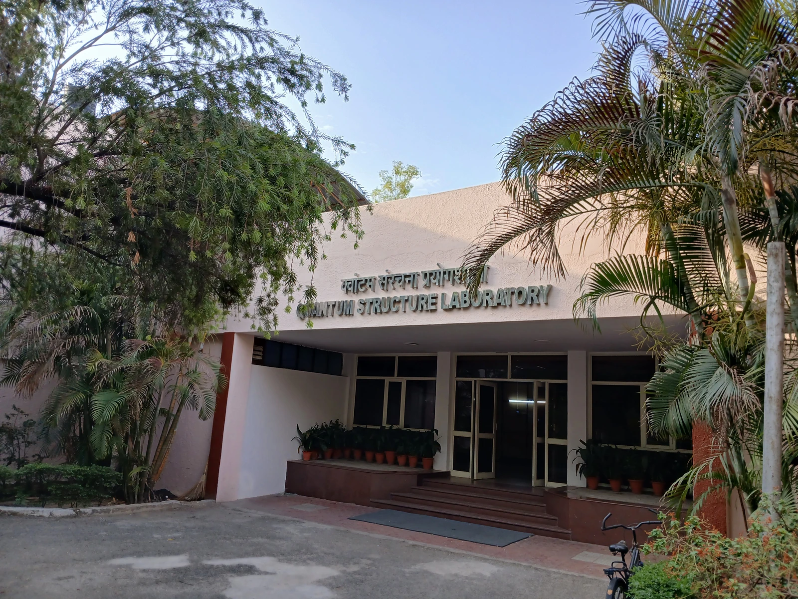
A quantum-structure laboratory from outside
CSIR-NPL’s Quantum Structure Laboratory in Delhi, photographed in June 2024. This existing QubitWire photograph is reused in the collection; Delhi is a different location from the IIT Mandi event venue.
Shishirdasika — Quantum structure laboratory in CSIR-NPL in Delhi.jpg — CC BY-SA 4.0 — https://commons.wikimedia.org/wiki/File:Quantum_structure_laboratory_in_CSIR-NPL_in_Delhi.jpg — https://creativecommons.org/licenses/by-sa/4.0.
Photographed 6 June 2024 · Archival photograph
Full original frame retained; EXIF orientation normalized where present, resized without enlargement and converted to WebP. No crop or content alteration.
Chapter 02
When light becomes a signal
A detector turns absorbed light into a measurable electrical response. These images show separate detector technologies and projects. Their performance has to be established by measurements.
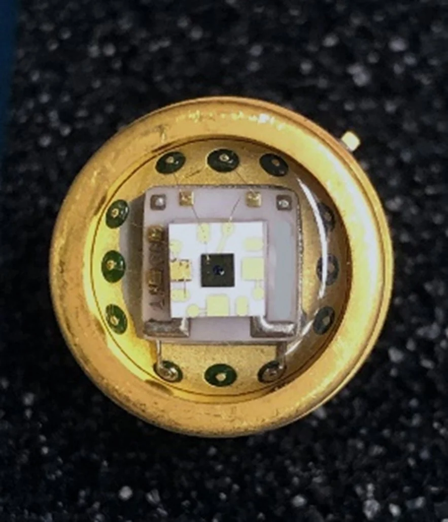
Single-photon avalanche diode
The round package surrounds a small single-photon avalanche diode and its connections. J. Bienfang/NIST photographed this commercial component; the January 2026 date belongs to the source upload.
J. Bienfang/NIST · NIST public information reuse terms
Capture date not established · Archival photograph
Proportional resizing and WebP re-encoding. No crop, compositing, recoloring or content removal. Original source and license retained.
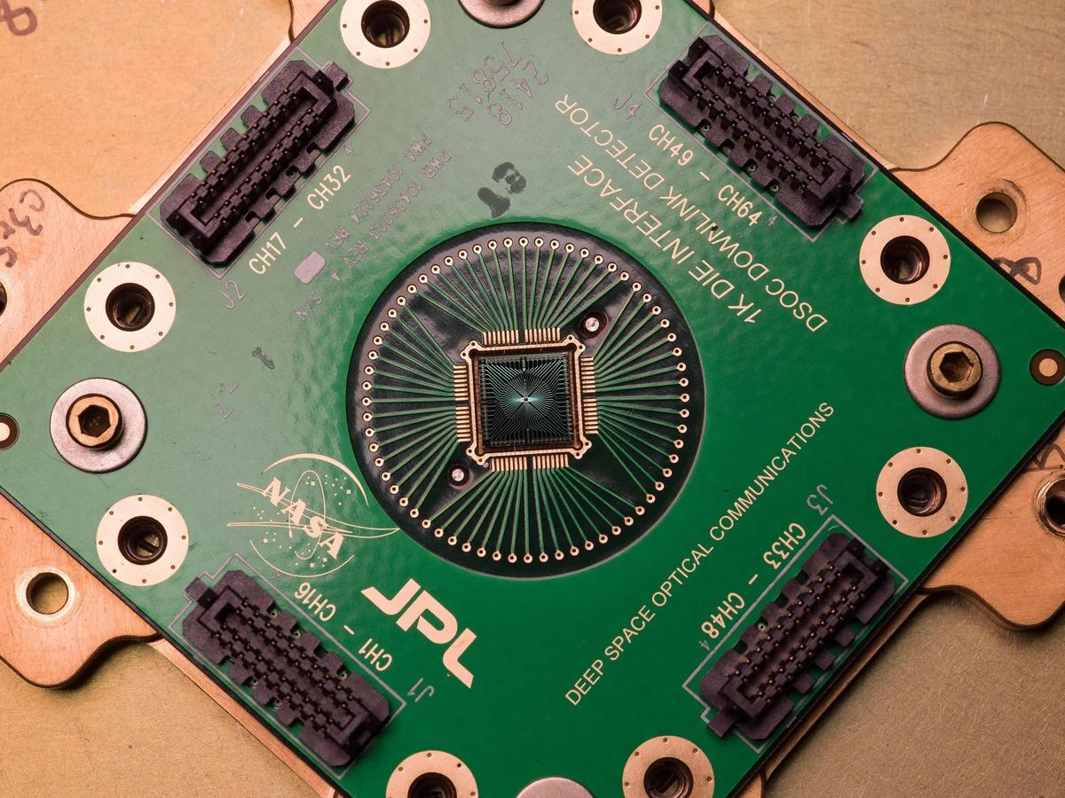
DSOC superconducting nanowire single-photon detector PIA26141
A detector built for NASA’s Deep Space Optical Communications demonstration sits at the centre of a green board. The October 2023 image shows an identical copy of the device used at Palomar Observatory, rather than a quantum-computing processor.
NASA/JPL-Caltech · Public domain (United States), NASA/JPL-Caltech image reuse terms
Photographed 4 October 2023 · Archival photograph
Proportional resizing and WebP re-encoding. No crop, compositing, recoloring or content removal. Original source and license retained.
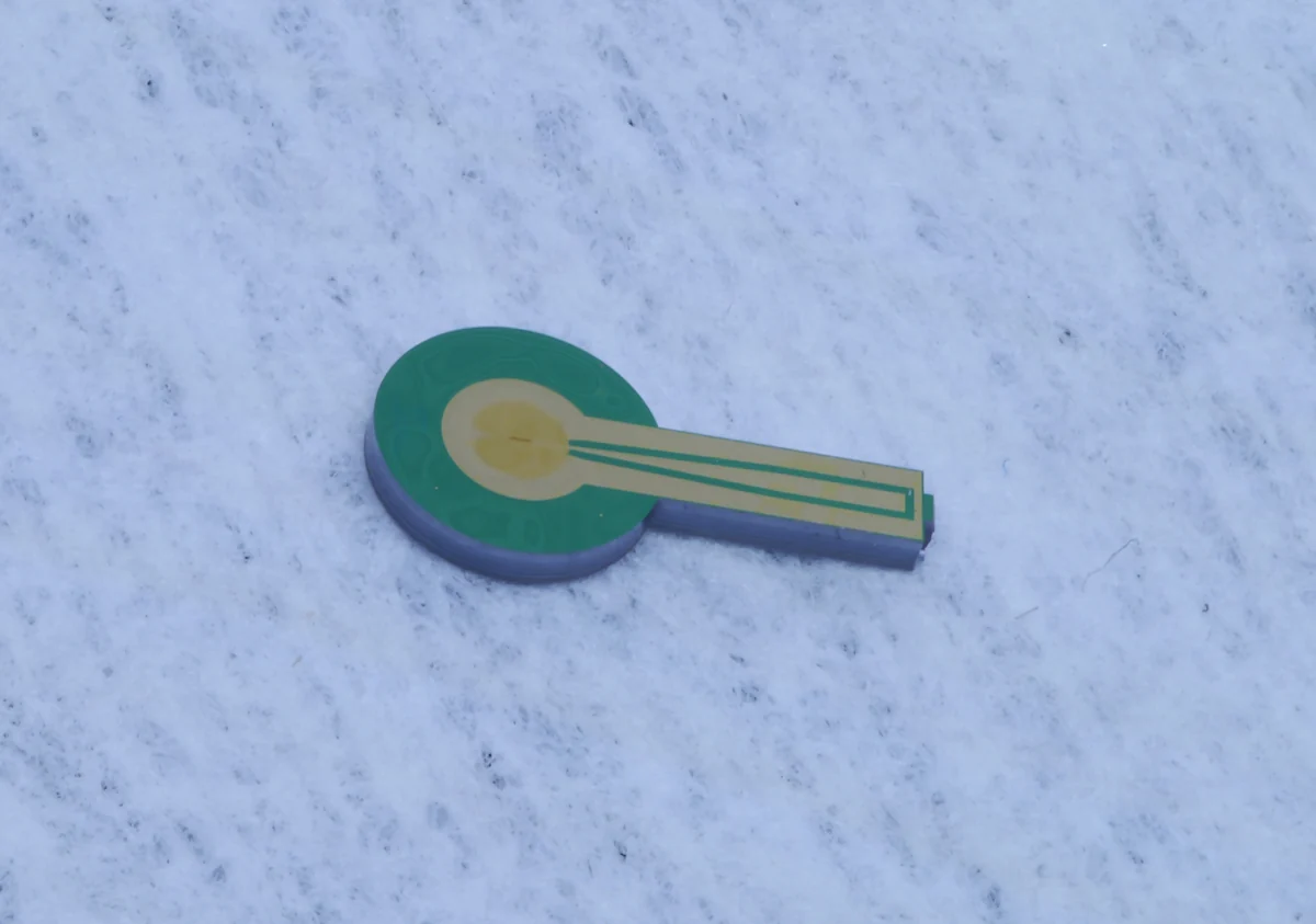
Single-Photon Detector - NIST chip
A compact superconducting nanowire detector chip photographed by Verma/NIST in September 2014. Its age remains visible when the image is used to explain photon-detection hardware.
Verma/NIST · NIST public information reuse terms
Photographed 15 September 2014 · Archival photograph
Proportional resizing and WebP re-encoding. No crop, compositing, recoloring or content removal. Original source and license retained.
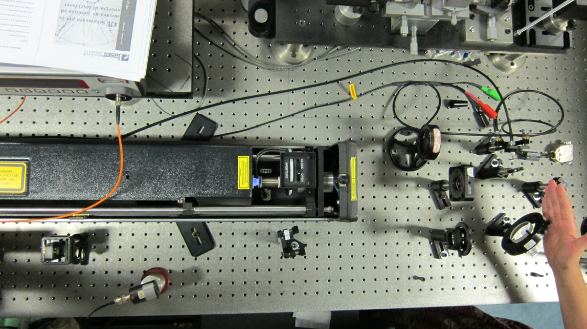
Optical table - Up view
An optical table photographed by Giorgio Brida in July 2010 makes the surrounding mirrors, mounts and connections visible. This is an archival view of optical work, separate from the detector projects beside it.
Giorgio Brida · CC BY 2.0
Photographed 30 July 2010 · Archival photograph
Proportional resizing and WebP re-encoding. No crop, compositing, recoloring or content removal. Original source and license retained.
Chapter 03
Measuring and connecting
Small devices depend on mounts, optics, wiring and controlled surroundings. These photographs and one labeled microscope image make those interfaces visible without treating them as evidence for a different laboratory’s result.
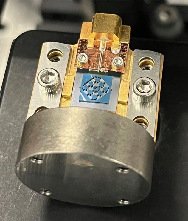
A flip-chip transducer cavity mount
The blue patterned transducer sits inside a metal cavity mount. This NIST photograph already appears in QubitWire’s gallery and is reused here with its existing identity. It is separate from IBM’s processor-link apparatus.
H. Le Corre/NIST — A flip-chip transducer cavity mount — Public domain in the United States; NIST worldwide reuse terms — https://www.nist.gov/programs-projects/quantum-transducer-design-and-fabrication — https://www.nist.gov/open/copyright-fair-use-and-licensing-statements-srd-data-software-and-technical-series-publications.
Capture date not established · Archival photograph
Full original frame retained; EXIF orientation normalized where present, resized without enlargement and converted to WebP. No crop or content alteration.
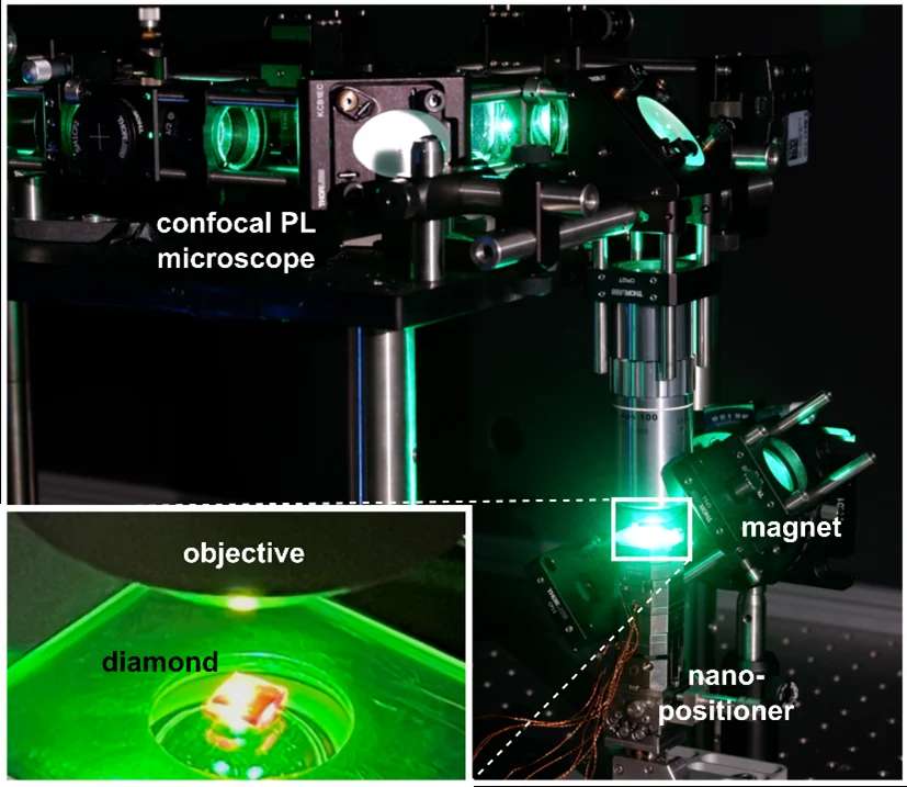
Quantum Diamond microscope
A quantum diamond microscope combines illumination, optics, a magnet and positioning hardware. The source labels are preserved in the full image so readers can identify those components.
NIST · NIST public information reuse terms
Capture date not established · Archival photograph
Proportional resizing and WebP re-encoding. No crop, compositing, recoloring or content removal. Original source and license retained.
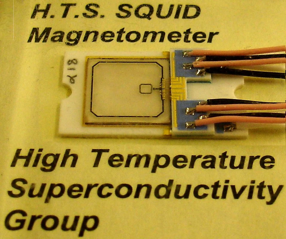
SQUID by Zureks
A historical SQUID sensing element photographed by Zureks and described as dating from 2008. It provides context for superconducting sensors rather than a view of a newly reported SQIF experiment.
Zureks · CC BY-SA 3.0
Photographed 2008 · Archival photograph
Proportional resizing and WebP re-encoding. No crop, compositing, recoloring or content removal. Original source and license retained. The adapted image remains available under CC BY-SA 3.0.
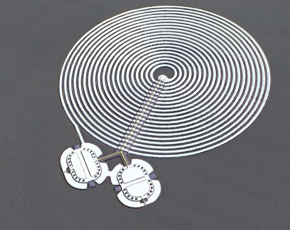
Quantum drums - wide microscope view
A microscope image shows two mechanical drums and their associated spiral circuit. NIST released the image in June 2023. The camera date is not established, and the image is labeled as a micrograph.
NIST · NIST public information reuse terms
Capture date not established · Archival micrograph
Proportional resizing and WebP re-encoding. No crop, compositing, recoloring or content removal. Original source and license retained.
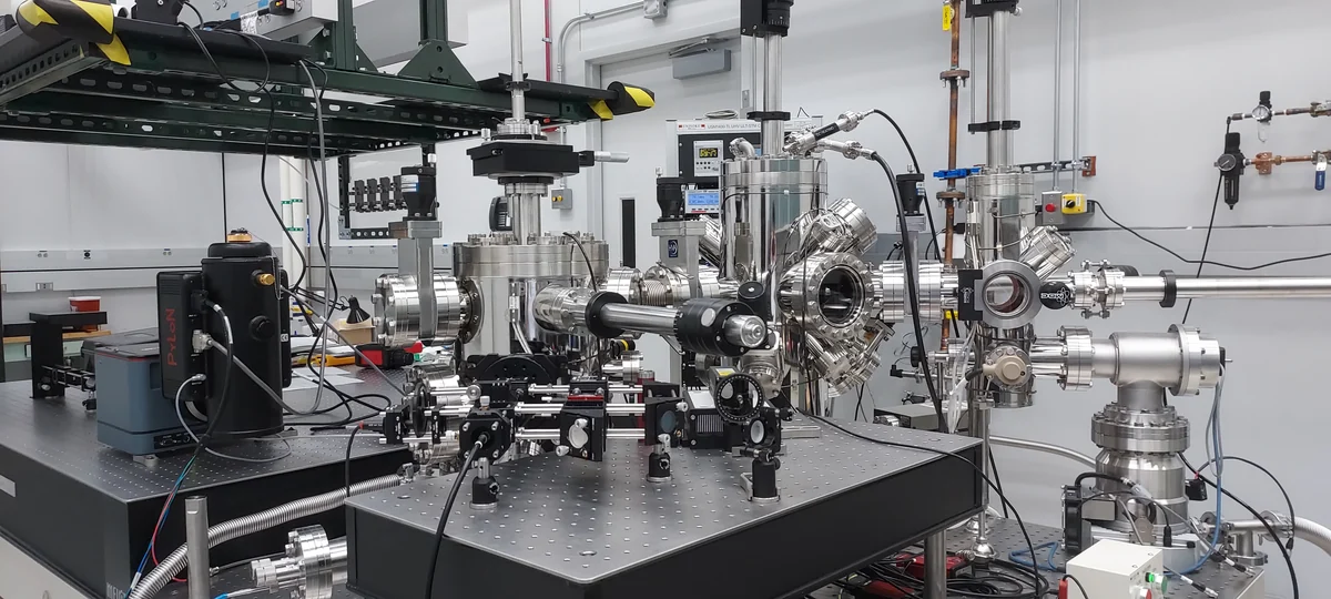
NIST ultrahigh vacuum (UHV) STM
NIST’s ultrahigh-vacuum scanning probe microscope platform fills a laboratory table with chambers, viewports and connections. This is measurement infrastructure, not a quantum processor or a newly commissioned UCLA refrigerator.
NIST · NIST public information reuse terms
Capture date not established · Archival photograph
Proportional resizing and WebP re-encoding. No crop, compositing, recoloring or content removal. Original source and license retained.